Introduction
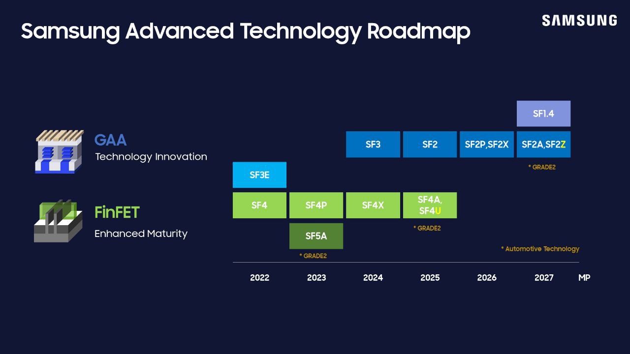
In a significant move, Samsung has unveiled its latest process technology roadmap at the Samsung Foundry Forum (SFF) U.S. event and the roadmap outlines the evolution of Samsung’s 2nm-class production nodes through 2027, highlighting advancements like backside power delivery and reaffirming the company’s commitment to introducing a 1.4nm-class node by 2027.
The introduction of a new high-value 4nm-class manufacturing technology further underscores Samsung’s strategic direction.
2nm-class production nodes by 2025: Their SF2 node (previously SF3P) boasts significant improvements in power, performance and density, rivaling 2nm-class process technologies. This positions Samsung to potentially lead TSMC in production timelines.
1.4nm-class node by 2027: Samsung plans to introduce an even more advanced 1.4nm-class production node by 2027.
Backside power delivery by 2027: Their SF2Z node, planned for 2027, will incorporate backside power delivery for enhanced performance and transistor density.
Background
The semiconductor industry is at the forefront of technological advancements, with leading companies constantly pushing the boundaries of what’s possible.
Historically dominated by companies like Intel, TSMC, and Samsung, the industry has seen intense competition and rapid innovation.
Samsung, a key player in this field, has been investing heavily in research and development to maintain its position as a leader in semiconductor technology.
Read More: Top 5 New design Tools and Software Transforming Semiconductor Design in 2024 – techovedas
Key Announcements
Samsung 2nm-Class Technologies
Samsung 2nm-class process technologies are central to the company’s latest roadmap. These technologies are set to enter production in 2025 and will be refined until 2027, when Samsung’s 1.4nm-class production node is expected to debut. Samsung has also introduced a new 2nm-class node, SF2, previously known as SF3P, aimed at high-performance devices.
“We have refined and improved the SF3P, resulting in what we now refer to as SF2. This enhanced node incorporates various process design improvements, delivering notable power, performance, and area (PPA) benefits,”
Samsung spokesperson.
Upcoming Process Nodes
Samsung announced several new process nodes planned for 2026 and 2027:
- SF2P (2026): A refinement of SF2, featuring faster yet less dense transistors.
- SF2Z (2027): Incorporates backside power delivery to improve power delivery quality and address voltage drop concerns.
Read More: Intel Partners with Sharp to Utilize Underused LCD Plants for Chip Research – techovedas
1.4nm-Class Node
Samsung’s 1.4nm-class node, slated for 2027, will not feature backside power delivery, setting it apart from other foundries. “We have optimized BSPDN and incorporated it for the first time in the SF2Z node we announced today. We will continue to refine this technology and apply it to future nodes, but we don’t have a specific timeline to share at this time,” explained a Samsung spokesperson.
Comparison with Competitors
Samsung’s roadmap aligns with other leading contract fabs regarding ‘nanometer’ designations. However, without further technical disclosures, the actual benefits and comparative advantages of each node remain uncertain.
Comparison of Leading-Edge Nodes
| Year | Intel Process | Samsung Process | TSMC Process |
|---|---|---|---|
| 2023 | Intel 3 | SF3E | N3E/N3P |
| 2024 | Intel 20A | SF3 | N3S/N3X |
| 2025 | Intel 18A | SF2 | N2 |
| 2026 | Intel 14A | SF2P/SF2X | A16 |
| 2027 | Intel 10A | SF2Z/SF1.4 | A14 (?) |
FET Technology and Power Delivery
- FET:
- Intel: RibbonFET (GAAFET)
- Samsung: GAAFET
- TSMC: FinFET to GAAFET transition
- Power Delivery:
- Intel: PowerVia (BSPDN)
- Samsung: Frontside, transitioning to Backside/?
- TSMC: Super Power Rail (BSPDN)
EUV Technology
- EUV:
- Intel: 0.33 NA EUV, 0.55 NA EUV + DSA
- Samsung: 0.33 NA EUV, future updates unclear
- TSMC: 0.33 NA EUV, future updates unclear
Read More: 5 Most Exciting Startups Building AI Hardware – techovedas
Significance
Samsung’s roadmap signifies a pivotal moment for the semiconductor industry. By advancing its process technologies and refining existing nodes, Samsung is poised to enhance power efficiency, performance, and area (PPA) benefits.
These developments are crucial as the demand for more powerful and efficient semiconductors grows, driven by applications in artificial intelligence, data centers, and advanced consumer electronics.
The introduction of backside power delivery in the SF2Z node addresses ongoing concerns about voltage drop, which is critical for maintaining the performance and reliability of modern chips.
This focus on power delivery highlights Samsung’s commitment to addressing real-world challenges faced by chip designers.
Read More: 5 Most Exciting Startups Building AI Hardware – techovedas
Conclusion
Samsung’s updated roadmap showcases the company’s dedication to pushing the boundaries of semiconductor technology.
By refining existing nodes and introducing new process technologies, Samsung aims to stay competitive in the rapidly evolving semiconductor industry.
The inclusion of backside power delivery and the emphasis on high-performance nodes reflect Samsung’s strategic focus on improving power efficiency and performance.
As the industry moves forward, it will be crucial to monitor how these advancements compare with those of competitors like Intel and TSMC.