The semiconductor industry is on the brink of a potential revolution as TSMC (Taiwan Semiconductor Manufacturing Company) embarks on an ambitious exploration of rectangular silicon wafers.
This innovative approach aims to significantly increase the usable area for chip production, addressing the growing demand for advanced multi-chiplet processors.
Instead of circles, rectangles: Traditionally, chip manufacturers like TSMC use circular silicon wafers to make chips. TSMC is now experimenting with rectangular “panel-like substrates” for advanced chip packaging.
More chips, less waste: These rectangular wafers are reported to measure 510 by 515 millimeters, offering over three times the usable area compared to the current 12-inch (300mm diameter) round wafers. This means more chips per wafer and less silicon wasted on the edges.
Why the change? Chip complexity is increasing, and the current round wafers might not be enough for future needs. Rectangular wafers could help meet the growing demand for powerful processors, especially for AI applications.
Early days yet: It’s important to note that this is still in the early stages. Developing and implementing this new method will require significant investment in new equipment and materials. It could be several years before we see widespread adoption of rectangular wafers.
Here, we delve into the details of this groundbreaking development, its challenges, and its potential impact on the semiconductor landscape.
Background: The Evolution of Semiconductor Wafers
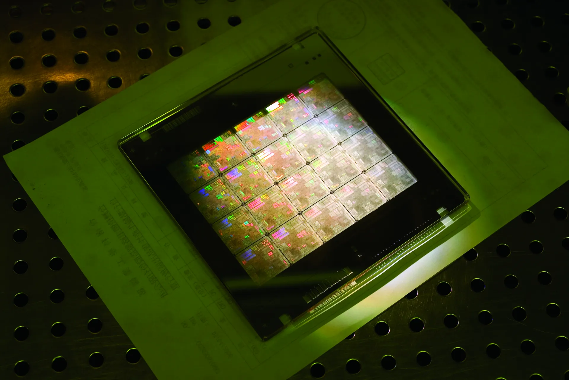
For decades, the semiconductor industry has relied on round silicon wafers with diameters evolving from 100mm to the current standard of 300mm.
These wafers have been the backbone of chip manufacturing, providing a well-balanced compromise between manufacturability, cost, and efficiency.
However, as technology advances and the complexity of chips increases, the limitations of these traditional wafers become more apparent.
The push for larger wafer sizes has been a continuous trend aimed at improving yield and reducing costs.
Each increase in wafer diameter has historically been associated with significant technological and economic challenges but ultimately resulted in substantial gains in production efficiency and cost-effectiveness.
Read More: Ilya Sutskever, Co-founder of OpenAI, Launches Startup to Tackle Safe Superintelligence – techovedas
TSMC’s Bold New Approach
TSMC is developing a new chip packaging method that leverages rectangular substrates measuring 510mm by 515mm. This new format offers approximately 3.7 times the usable area of the conventional 300mm round wafers.
The increased surface area allows for more chips to be produced per wafer, thereby reducing the waste typically associated with the edges of round wafers. This shift could lead to significant efficiency gains and cost savings in chip production.
Read More :$2 Billion Boost: Onsemi Ambitious Expansion in Czech Republic – techovedas
Why It Matters: The Growing Demand for Advanced Chips
The semiconductor industry is experiencing unprecedented demand driven by advancements in artificial intelligence, high-performance computing, 5G technology, and other cutting-edge fields.
As chips become more complex and powerful, the need for efficient and scalable manufacturing processes has never been greater.
Traditional wafer sizes and shapes are becoming less efficient for these advanced applications, necessitating innovative solutions like TSMC’s rectangular wafers.
Technical and Financial Hurdles
Transitioning to rectangular wafers is not without its challenges. The existing manufacturing infrastructure is heavily optimized for 300mm round wafers.
The shift to rectangular substrates requires entirely new equipment and significant modifications to production processes.
Precision is critical in semiconductor manufacturing, and adapting current tools and materials to the new substrate shape presents a considerable challenge.
Financially, the transition demands a substantial upfront investment. TSMC will need to overhaul its facilities, including upgrades to robotic arms, automated material handling systems, and other critical infrastructure. Despite the high costs, TSMC’s substantial resources and industry leadership position it well to drive this innovation forward.
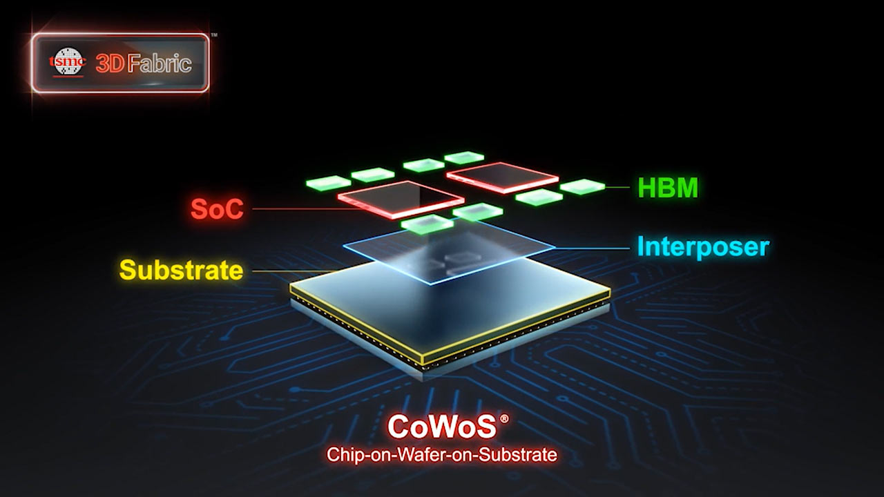
Current Advanced Packaging Techniques
TSMC is a leader in advanced packaging technologies, with methods like CoWoS (chip-on-wafer-on-substrate) playing a crucial role in producing high-performance AI processors for clients such as Nvidia, AMD, Amazon, and Google.
These techniques utilize 300mm wafers and are essential for meeting the demands of increasingly complex AI chips.
However, as these chips grow in size and complexity, the efficiency of existing methods may decline, highlighting the need for a new approach.
Industry Collaboration and Long-Term Vision
The development of rectangular wafer technology is still in its early stages and could take five to ten years to commercialize.
During this period, TSMC is working closely with equipment and material suppliers to develop the necessary tools and processes. The company’s collaboration with these partners is critical to overcoming the technical challenges associated with the new substrate format.
TSMC’s long-term vision underscores its commitment to maintaining its leadership in semiconductor innovation. By pushing the boundaries of current manufacturing techniques, TSMC aims to set new industry standards and ensure its continued dominance in the market.
Read More:ASICs vs. FPGAs: Choosing the Right Technology for Your Design – techovedas
Significance: Transforming the Semiconductor Landscape
If successful, TSMC’s transition to rectangular silicon wafers could have a profound impact on the semiconductor industry. The increased wafer area will enable higher chip yields per wafer, reducing production costs and potentially lowering prices for consumers. Additionally, the reduction in edge waste aligns with the industry’s push towards more sustainable manufacturing practices.
This innovation could also accelerate the development of next-generation technologies, including artificial intelligence, high-performance computing, and advanced telecommunications. By enhancing the efficiency and capacity of chip production, TSMC’s initiative could drive significant advancements in these fields.
Read More :$2 Billion Boost: Onsemi Ambitious Expansion in Czech Republic – techovedas
Conclusion
TSMC’s exploration of rectangular silicon wafers represents a bold and visionary approach to addressing the limitations of current semiconductor manufacturing techniques.
While the transition poses significant technical and financial challenges, the potential benefits in terms of efficiency, cost reduction, and technological advancement are substantial.
As the world’s largest contract chipmaker, TSMC is well-positioned to lead this transformative shift. The coming years will be crucial in determining whether this ambitious plan will come to fruition, but one thing is certain: TSMC’s relentless pursuit of innovation continues to push the boundaries of what is possible in the semiconductor industry.