Introduction
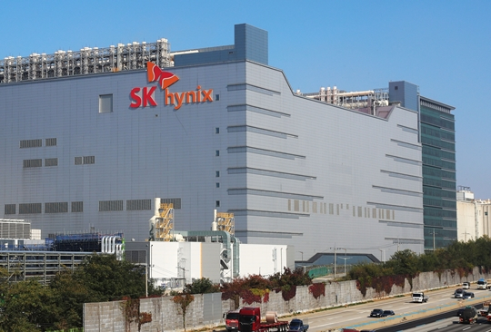
In the realm of technological advancements, memory storage plays a pivotal role in shaping the capabilities of various devices, from smartphones to data centers. South Korean semiconductor giant SK Hynix is once again at the forefront of innovation, introducing its groundbreaking 321-layer 1 terabyte (TB) TLC 4D NAND Flash memory chips. Unveiled at the Flash Memory Summit (FMS) 2023 in Santa Clara, USA, these chips represent a significant leap forward in storage density, performance, and efficiency. In this blog post, we’ll delve into the details of this cutting-edge technology, its benefits, and its potential applications across various industries.
The Evolution of Flash Memory
Flash memory technology has evolved rapidly over the years, enabling the storage of increasingly larger amounts of data in ever-shrinking form factors. SK Hynix’s latest achievement, the 321-layer 1 Tb 4D NAND chips, signifies a major milestone in this ongoing journey of innovation.
Unveiling the 321-Layer 1Tb 4D NAND Chips
SK Hynix’s 321-layer 1 Tb TLC 4D NAND Flash memory chips are poised to revolutionize the storage landscape with their remarkable features. One of the most striking attributes is the immense storage density – a 59% increase per chip compared to the previous generation of 238-layer 512 Gb chips. This means that devices incorporating these chips, such as Solid State Drives (SSDs), will be able to store substantially more data without compromising on physical dimensions.
The key to achieving this boost in storage density lies in the innovative stacking of memory cells within the chip. By utilizing a 4D NAND architecture and the new CMOS-under-array design, SK Hynix has managed to maximize the use of space while ensuring efficient cell stacking. This approach not only increases storage capacity but also contributes to enhanced performance and efficiency.
Performance and Efficiency
Apart from the increase in storage density, the 321-layer 1 Tb 4D NAND chips also deliver impressive performance metrics. With a read speed of up to 1.6 gigabits per second (GB/s) and a write speed of up to 1.2 GB/s, these chips are well-equipped to handle data-intensive applications. This performance boost is particularly advantageous for high-end smartphones, servers, data centers, and other environments where rapid data access and transfer are crucial.
Moreover, the new NAND chips exhibit a lower power consumption, which is up to 30% lower than previous generations. This reduction in power usage not only enhances device battery life but also contributes to a greener and more sustainable technological landscape.
Applications across Industries
The impact of SK Hynix’s 321-layer 1 Tb 4D NAND chips extends far beyond consumer electronics. Industries ranging from automotive to medical are poised to benefit from this cutting-edge technology.
- High-end Smartphones: The increased storage capacity and high-performance attributes make these NAND chips ideal for flagship smartphones, catering to users who demand both ample storage for multimedia content and seamless app performance.
- Data Centers and Servers: In the era of big data and cloud computing, the need for high-speed, high-capacity storage solutions is paramount. SK Hynix’s NAND chips can significantly enhance the performance of data centers and servers, ensuring efficient data handling and processing.
- Automotive and Industrial: With the rise of connected vehicles and Industry 4.0, there’s a growing demand for reliable, high-capacity storage in automotive and industrial applications. These NAND chips can provide the necessary storage for critical systems and applications.
- Medical: In the medical field, where data accuracy and accessibility are crucial, these NAND chips can facilitate the storage and retrieval of medical records, imaging data, and more.
Looking Forward: Technological Leadership
SK Hynix’s commitment to innovation is evident in its consistent efforts to release new NAND memory chip generations every two years. This strategy not only solidifies the company’s technological leadership but also ensures that it remains at the forefront of meeting the evolving demands of the AI era.
Conclusion
The unveiling of SK Hynix’s 321-layer 1 Tb 4D NAND chips marks a significant milestone in flash memory technology. The increased storage density, enhanced performance, lower power consumption, and diverse applications underscore the transformative potential of this innovation. As mass production is projected to commence in the first half of 2025, we can anticipate a new era of devices and systems empowered by this groundbreaking technology. SK Hynix’s commitment to pushing the boundaries of what’s possible in memory storage sets the stage for a future where data-intensive applications are seamlessly supported, opening doors to untold possibilities across industries.