Introduction
In the realm of modern technology, semiconductor play a pivotal role, serving as the cornerstone of electronic devices. These tiny, yet powerful components, typically manufacturing from silicon or germanium, have revolutionized the way we live, work, and communicate.
Their ability to amplify, switch, and process electrical signals has enabled the development of a vast array of electronic devices, from computers and smartphones to medical equipment and industrial machinery.
Let’s delve even deeper into each step of semiconductor manufacturing, providing a more comprehensive overview:
Wafer Preparation:
The journey starts by preparing silicon wafers, which serve as the foundation for building semiconductor devices. Typically, these wafers have a diameter of 300 millimeters, and manufacturers slice them from a silicon ingot. Following this, they polish the wafers to achieve an extremely smooth surface, creating an impeccable canvas for subsequent steps.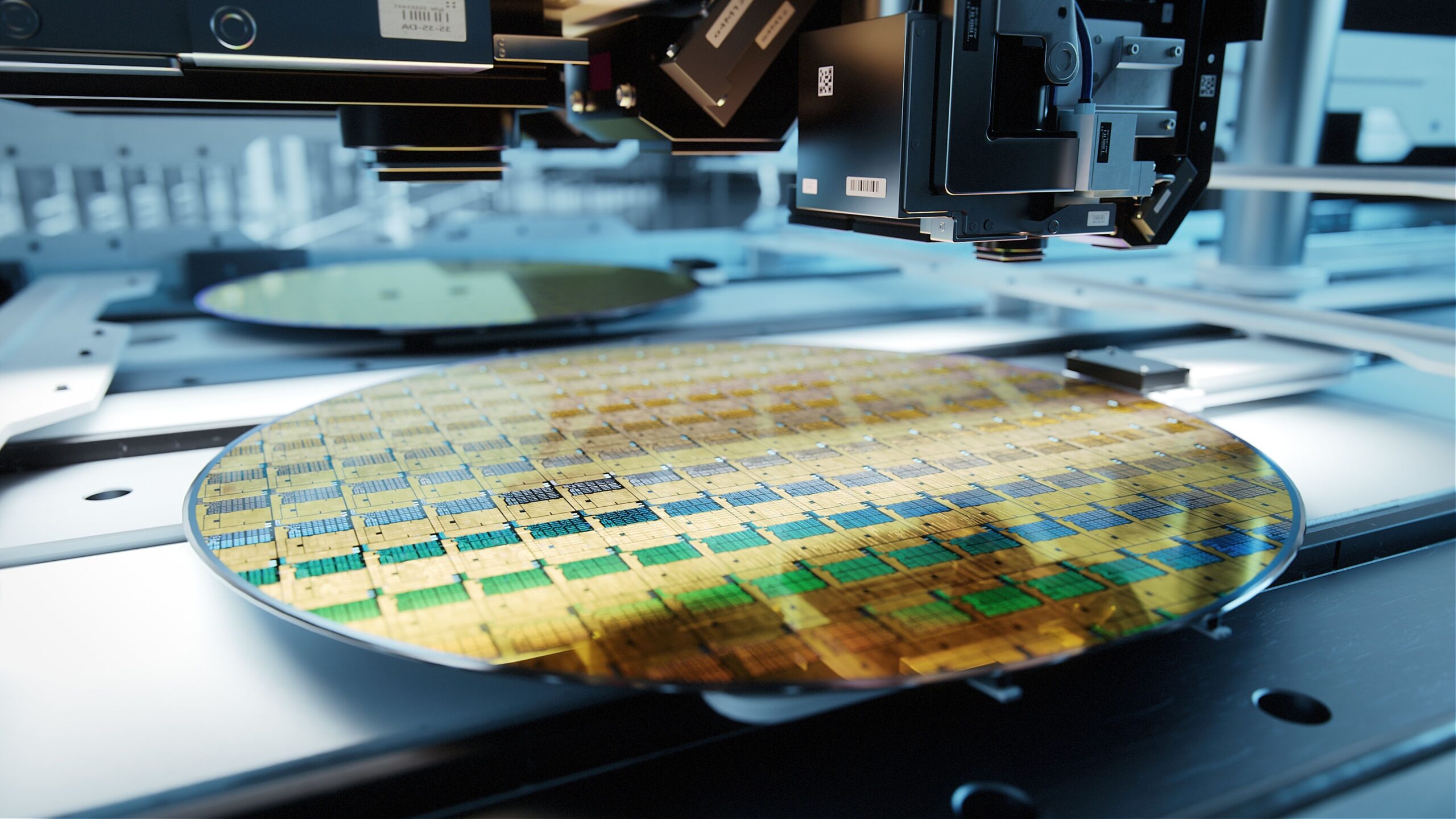
Rigorous testing examines silicon wafers for defects, and chemical and mechanical processes remove any impurities. The wafers undergo precise slicing and polishing to achieve an ultra-smooth surface. Frequently, manufacturers deposit a thin layer of oxide or nitride to insulate and protect the silicon wafers.
Importance: Wafer quality is paramount, as it sets the stage for flawless semiconductor device fabrication.
Read More: 15 Top Semiconductor companies in the World – techovedas
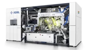
Lithography:
The intricate patterns of transistors and other circuit elements are transferred onto the wafer using a process called lithography. This involves coating the wafer with a photosensitive material called photoresist, exposing it to ultraviolet light through a mask, and then developing the resist to reveal the desired patterns.
Lithography involves multiple steps. Apply a photoresist to the wafer, expose it to light through a mask with the desired circuit pattern, and chemically treat it to develop the pattern. Advanced techniques like electron-beam and EUV lithography offer enhanced precision for smaller feature sizes.
Importance: The accuracy and resolution of lithography dictate the intricacy and density of the semiconductor circuitry.
Etching:
The exposed areas of the wafer are then selectively removed using a process called etching. This involves either wet etching, using chemicals to dissolve the unwanted material, or dry etching, using plasma or ions to bombard and remove the material. The remaining patterns form the physical structures of the semiconductor devices.
Etching processes, whether wet or dry, are meticulously controlled. Wet etching utilizes chemical solutions to selectively remove material, while dry etching uses plasma or ions for more precise material removal. Multiple etching steps may be employed to create different structures.
Importance: Etching defines the three-dimensional structures of transistors, interconnects, and other components on the wafer.
Doping:
Intentionally introduce impurities into the silicon material to impart the desired electrical properties through a process called doping. This involves diffusing or implanting dopant atoms into the wafer, altering the conductivity of the semiconductor and enabling it to conduct electricity.
Introduce dopant atoms, such as phosphorus or boron, into the silicon wafer through diffusion or implantation. Precise control of doping levels and distribution is critical for creating regions with specific electrical properties.
Importance: Doping transforms the semiconductor material into regions with varying conductivity, enabling the formation of essential electronic components.
Metallization:
Form a network of metal conductors on the wafer using the metallization process. This involves depositing thin layers of conductive metals, such as aluminum or copper, using techniques like physical vapor deposition (PVD) or chemical vapor deposition (CVD). These metal layers connect the various components of the semiconductor device.
Metal deposition involves techniques like physical vapor deposition (PVD) or chemical vapor deposition (CVD) to create conductive layers. Apply a barrier layer, often made of titanium or tantalum, first, followed by depositing copper or aluminum.
Importance: Metallization establishes the electrical interconnections between various semiconductor components, forming the intricate circuitry.
Read More: Texas Instruments Breaks Ground on $11 Billion 300mm Wafer Fab in USA – techovedas
Passivation:
Deposit a thin layer of passivating material on the wafer to protect the semiconductor device from environmental contaminants. This layer, often made of silicon nitride or another protective material, prevents corrosion and oxidation, ensuring the long-term reliability of the device.
Passivation layers, typically made of silicon dioxide, nitride, or a combination, are applied to protect the semiconductor from environmental factors, including moisture and contaminants. Chemical treatments ensure a uniform and effective passivation layer.
Importance: Passivation enhances the reliability and longevity of semiconductor devices by preventing environmental damage.
Dielectrics:
To isolate the metal conductors and prevent short circuits, a layer of dielectric material is deposited on the wafer. This layer, typically made of silicon dioxide or another insulating material, ensures that electrical signals flow through the intended paths.
Strategically deposit dielectrics, such as silicon dioxide or hafnium oxide, to insulate and separate different layers of circuitry. Precise control over dielectric thickness is crucial to avoid electrical interference.
Importance: Dielectrics play a pivotal role in preventing unwanted electrical interactions, enabling the proper functioning of individual semiconductor components.
Packaging:
Encapsulate the individual semiconductor chips in protective packages to shield them from physical damage and environmental contaminants.This packaging process involves attaching the chip to a lead frame that provides electrical connections and enclosing it in a protective casing made of epoxy or ceramic.
Packaging involves encapsulating the semiconductor device in a protective casing, often using materials like ceramics or plastics. Establish electrical connections using wire bonding or flip-chip techniques, and seal the package to shield the device from external elements.
Importance: Proper packaging ensures the durability, reliability, and thermal performance of the semiconductor device in real-world applications.
Testing
Testing: The final step involves rigorous testing of the packaged semiconductor chips to ensure they meet the desired performance specifications. This involves electrical testing, functional testing, and environmental testing to verify the chip’s functionality, reliability, and ability to withstand various operating conditions.
 Semiconductor testing ensures quality and functionality throughout manufacturing. Wafer testing identifies defects early, burn-in tests assess device endurance, and final testing verifies specifications. System-level and functional testing evaluate integrated and operational aspects. Reliability testing predicts long-term performance. Quality control and failure analysis ensure consistent quality, and packaging completes the process.
Conclusion
The intricate process of semiconductor manufacturing, spanning multiple steps and involving specialized equipment and techniques, has revolutionized the electronics industry and enabled the creation of devices that have transformed our lives. From the microprocessors that power our computers to the sensors that enable smartphones to function, these tiny components play a vital role in shaping our modern world.