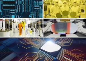
Introduction
Transistors are fundamental components in the world of modern electronics, acting as the essential switches and amplifiers in countless devices. Since their invention, transistors have revolutionized technology, enabling the development of everything from simple gadgets to complex computer systems. This article provides an in-depth look at 5 types of transistors widely used in today’s semiconductor industry. By understanding the unique characteristics and applications of each type, we can appreciate how these tiny components power the vast array of technological advancements we rely on daily.
Read More: Why GlobalFoundries Abandoned the Sub-7 nm Race: A Detailed Analysis – techovedas
Background of Types of Transistors
Transistors are the building blocks of modern electronic devices, essential for amplifying and switching electronic signals in a wide array of applications. Since the invention of the first transistor in 1947, the technology has evolved significantly, leading to the development of various types of transistors, each optimized for specific performance characteristics and applications. From the classic Bipolar Junction Transistor (BJT) to the advanced Fully Depleted Silicon-On-Insulator (FD-SOI) transistors, these devices have played a crucial role in the miniaturization and enhancement of electronic circuits.
In this blog post, we will explore the detailed structure, operation, advantages, disadvantages, and applications of different types of transistors, including BJTs, Metal-Oxide-Semiconductor Field-Effect Transistors (MOSFETs), Fin Field-Effect Transistors (FinFETs), Tunnel Field-Effect Transistors (TFETs). Each type offers unique benefits that cater to specific technological needs, contributing to the continuous advancement of electronics and paving the way for future innovations.
5 Types of Transistors Used in Modern Semiconductor Industry: Advantages & Applications
1. Bipolar Junction Transistors (BJTs)

Structure
- Layers: BJTs consist of three layers of semiconductor material, forming two p-n junctions. They are classified into NPN and PNP types.
- Terminals: They have three terminals: emitter, base, and collector.
- Regions: The emitter is heavily doped to inject charge carriers, the base is thin and lightly doped to allow carriers to pass through, and the collector is moderately doped to collect the carriers.
Operation
- Charge Carrier Injection: In NPN transistors, electrons are injected from the emitter into the base, and in PNP transistors, holes are injected. The base current controls the larger collector current.
- Amplification: Small changes in the base current result in large changes in the collector current, allowing the transistor to amplify signals.
Advantages
- High Gain: BJTs can provide high current and voltage gain.
- Analog Applications: Well-suited for analog circuits and linear amplification.
Disadvantages
- Power Consumption: Higher power consumption compared to MOSFETs due to continuous current flow through the base.
- Switching Speed: Slower switching speed compared to MOSFETs, limiting their use in high-frequency applications.
Applications
- Analog Circuits: Used in amplifiers, oscillators, and audio devices.
- Switching: Employed in switching applications where linearity is not a primary concern.
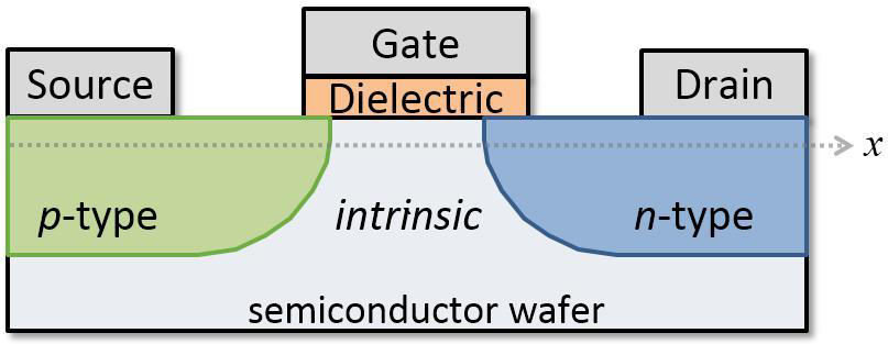
2. Metal-Oxide-Semiconductor Field-Effect Transistors (MOSFETs)

N and P Channel MOSFETs
Structure
- Layers: MOSFETs have a gate, source, and drain terminal. The gate is separated from the channel by a thin oxide layer.
- Types: They come in N-channel (NMOS) and P-channel (PMOS) varieties, with complementary pairs forming CMOS technology.
Operation
- Electric Field Control: Applying a voltage to the gate creates an electric field that modulates the conductivity of a channel between the source and drain.
- High Input Impedance: The gate is insulated, resulting in very high input impedance and low power consumption.
Advantages
- Low Power Consumption: Insulated gate results in negligible gate current, reducing power consumption.
- High Speed: Capable of high-speed operation, making them suitable for digital circuits.
Disadvantages
- Leakage Current: Subthreshold leakage current can be an issue, especially in modern, scaled-down devices.
- Sensitivity: Sensitive to static discharge and overvoltage, requiring careful handling.
Applications
- Digital Circuits: Widely used in microprocessors, memory devices, and other digital ICs.
- Analog Applications: Employed in analog switches, amplifiers, and voltage regulators.
Read More: $18 billion USD: South Korea Unveils Semiconductor Ecosystem Support Package – techovedas
3. Fin Field-Effect Transistors (FinFETs)

Structure
- 3D Structure: FinFETs have a thin, fin-like channel that rises above the substrate, with the gate wrapping around the fin on three sides.
- Improved Control: The 3D structure enhances the gate’s control over the channel, reducing short-channel effects.
Operation
- Better Electrostatic Control: The wrap-around gate provides better control over the channel, improving performance and reducing leakage currents.
- Higher Density: The 3D structure allows for higher transistor density on a chip.
Advantages
- Reduced Leakage: Improved control over the channel reduces leakage currents.
- High Performance: Enhanced electrostatic control leads to better performance, especially at smaller geometries.
Disadvantages
- Complex Manufacturing: The 3D structure is more complex to manufacture, increasing fabrication costs.
- Thermal Management: Managing heat dissipation can be more challenging due to the higher density.
Applications
- Advanced Processors: Used in high-performance processors and other advanced digital circuits.
- Mobile Devices: Employed in mobile SoCs where power efficiency and performance are critical.
4. Fully Depleted Silicon-On-Insulator (FD-SOI) Transistors
FD-SOI is a type of MOSFET that incorporates a silicon-on-insulator structure with a thin, fully depleted silicon layer.
Structure
- SOI Wafer: FD-SOI transistors are built on an SOI wafer, which consists of a thin layer of silicon separated from the bulk substrate by a buried oxide (BOX) layer.
- Fully Depleted Channel: The silicon layer is thin enough to be fully depleted of charge carriers, which enhances the control of the gate over the channel.
- Gate: The gate electrode is placed on top of a thin oxide layer, similar to conventional MOSFETs.
Operation
- Reduced Leakage: The fully depleted channel reduces leakage currents, which is critical for low-power applications.
- Improved Performance: FD-SOI transistors offer better electrostatic control of the channel, leading to improved performance and reduced short-channel effects.
- Body Biasing: FD-SOI technology allows for dynamic control of the transistor’s threshold voltage through body biasing. By adjusting the voltage applied to the substrate, one can optimize the threshold voltage, enhancing performance and reducing power consumption.
Advantages
- Lower Power Consumption: Reduced leakage currents and better control over the channel lead to lower power consumption.
- High Performance: Enhanced electrostatic control and reduced short-channel effects improve performance, making FD-SOI suitable for high-speed applications.
- Design Flexibility: The ability to adjust threshold voltage through body biasing provides flexibility in balancing power and performance.
Applications
- Mobile Devices: FD-SOI transistors are used in mobile processors and System-on-Chip (SoC) designs where power efficiency is crucial.
- Internet of Things (IoT): Low-power and high-performance characteristics make FD-SOI ideal for IoT applications.
- Automotive: FD-SOI technology is employed in automotive electronics for its reliability and power efficiency.
5. Tunnel Field-Effect Transistors (TFETs)
Structure
- Tunneling Junction: TFETs have a tunneling junction where quantum tunneling is used to switch the transistor on and off.
- Low Doping: The source and drain regions are lightly doped compared to traditional FETs.
Operation
- Quantum Tunneling: Switching is achieved through quantum tunneling of carriers across the barrier, rather than thermal injection.
- Low Voltage Operation: Can operate at lower voltages compared to MOSFETs, reducing power consumption.
Advantages
- Ultra-Low Power: Extremely low power consumption due to low operating voltage and leakage currents.
- Steep Subthreshold Slope: Provides a steeper subthreshold slope than MOSFETs, enabling better control of the off-state current.
Disadvantages
- Lower Drive Current: The drive current is typically lower than that of MOSFETs, which can limit performance.
- Complex Fabrication: More challenging to fabricate due to the need for precise control of the tunneling junction.
Applications
- Low-Power Devices: Ideal for ultra-low power applications such as wearable electronics and IoT devices.
- Energy-Efficient Computing: Used in energy-efficient computing where power consumption is critical.
Follow us on Linkedin for everything around Semiconductors & AI
Conclusion
Transistors are the cornerstone of modern electronics, enabling the rapid advancements in technology we witness today. The Types of Transistors, from Bipolar Junction Transistors (BJTs) to cutting-edge Graphene Transistors, reflects the ongoing efforts to optimize performance, reduce power consumption, and increase device density. Each type of transistor, with its unique structure and operational characteristics, offers specific advantages that make it suitable for particular applications.
BJTs, with their high current and voltage gain, remain integral in analog circuits. MOSFETs, with their low power consumption and high speed, dominate digital circuits and microprocessors. FinFETs offer enhanced control and reduced leakage, making them ideal for advanced digital applications. TFETs promise ultra-low power consumption for energy-efficient devices.
The development and integration of these transistors continue to drive innovation in fields ranging from consumer electronics to automotive and healthcare. Understanding the intricacies of each transistor type allows engineers and designers to choose the best components for their specific needs, ensuring the continued evolution of technology. As we look to the future, the exploration of new materials and structures will undoubtedly lead to even more sophisticated and efficient transistors, further expanding the horizons of what is possible in electronics.