
Introduction
In a world where communication is the cornerstone of progress, the quest for faster, more reliable data transmission methods is unending. Enter the groundbreaking innovation emerging from the laboratories of Wuhan, China – a cost-effective chip that promises to simplify the manufacturing process of high-performance photonic devices.
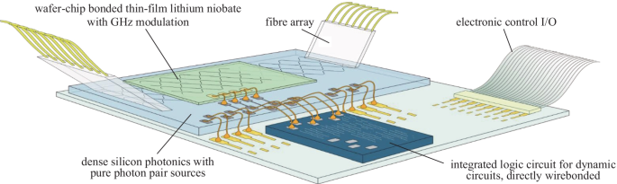
Chinese researchers developed a new type of chip that simplifies the process of making high-performance photonic devices. These devices use light signals to transmit data, potentially offering much faster communication speeds than traditional methods. The key to this innovation is a technique that bonds two different types of wafers together, creating a more efficient device for transmitting and receiving light signals.
Spearheaded by researchers at the JFS Laboratory. It’s a significant leap forward in telecommunications. Promises to revolutionize industries. From 5G wireless communication to aerospace engineering.
Follow us on Linkedin for everything around Semiconductors & AI
The Power of Wafer Bonding: A Milestone Achievement
The innovation described revolves around a technique called “wafer bonding” and its application in combining an 8-inch silicon photonics wafer with a lithium niobate wafer. Here’s a breakdown of the components and their significance:
Wafer Bonding: This is a process where two semiconductor wafers are joined together, typically at the atomic or molecular level, to create a single integrated structure. It’s a crucial technique in semiconductor manufacturing for creating complex devices.
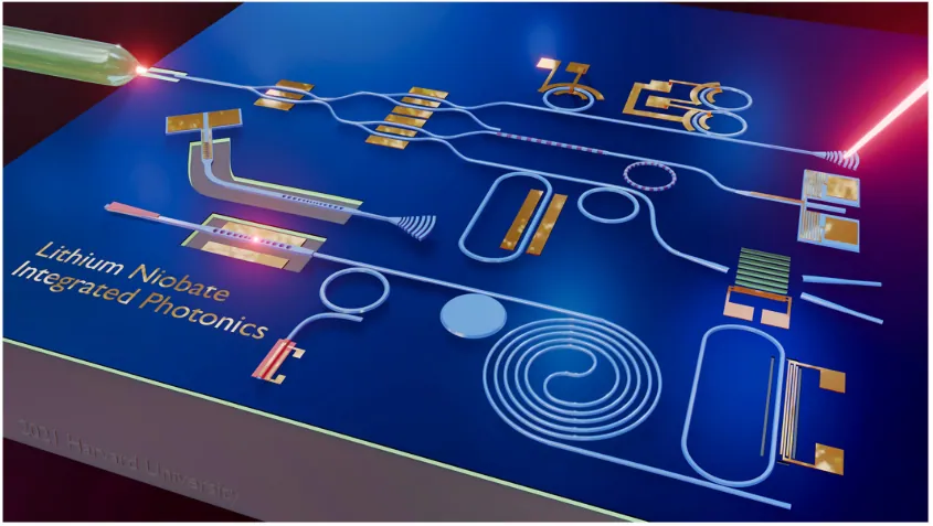
Silicon Photonics Wafer: Silicon photonics involves the use of silicon as a medium for generating, guiding, modulating, and detecting light signals. Silicon is widely used in the electronics industry due to its compatibility with existing manufacturing processes and its ability to integrate with electronic components.
Lithium Niobate Wafer: Lithium niobate, a crystalline material renowned for its exceptional electro-optic properties, efficiently converts electrical signals into optical signals (light) and vice versa. It finds widespread application in telecommunications, photonics, and other high-speed optical communication systems.
By bonding these two wafers together, researchers have created a hybrid structure that leverages the strengths of both materials:
Efficient Light Transmission: Silicon photonics enables efficient generation and manipulation of light signals within the silicon material. Meanwhile, lithium niobate offers excellent electro-optic properties, enabling efficient modulation and detection of light signals.
High Electro-Optical Performance: The combination of silicon photonics and lithium niobate results in a device capable of achieving high electro-optical performance. This means it can efficiently transmit and receive data-carrying light signals with minimal loss or distortion, making it ideal for applications requiring high-speed and high-bandwidth data communication.
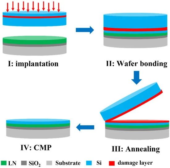
Image Credits: MDPI
The implications of this achievement are significant:
Advanced Communication Systems: The new device could lead to the development of advanced communication systems capable of handling massive amounts of data with greater efficiency and speed. This could benefit various sectors such as telecommunications, data centers, and internet infrastructure.
Optical Computing: The integration of silicon photonics with lithium niobate opens up possibilities for optical computing, where light signals are used for processing and transmitting data, potentially leading to faster and more energy-efficient computing systems.
Sensor Technologies: The device could also find applications in sensor technologies, where high-speed and high-resolution sensing capabilities are required. This includes medical imaging, environmental monitoring, and industrial automation.
Versatile Applications: Transforming Industries
This breakthrough streamlines 5G wireless communication, ensuring faster, reliable connections. It meets modern connectivity demands. Impact extends to optical communication, enabling efficient, cost-effective solutions.
Industries like aerospace benefit greatly. Enhanced photonic device capabilities enable data transmission in challenging environments, opening new possibilities.
Read More: MediaTek beats Apple as the Top Smartphone Chip Vendor in 2023
Advantages of Light Signals: The Superior Choice
But what sets light signals apart and makes them superior for communication compared to other methods? The answer lies in several key advantages:
Speed: Light travels at an incredibly fast pace, far surpassing the speed of electricity. This enables much quicker data transmission over long distances, essential for applications where speed is of the essence.
Capacity: Light signals have the ability to carry a substantially larger volume of data compared to electrical signals. This high bandwidth capacity makes them ideal for applications requiring intensive data transmission.
Immunity: Unlike electrical signals, light signals are immune to electromagnetic interference. This inherent immunity ensures reliable data transfer even in the presence of external disturbances. This makes it suitable for operation in harsh environments.
Distance: Light signals experience minimal signal degradation over long distances, making them an ideal choice for long-haul communication networks. This characteristic ensures that data can be transmitted reliably over extended geographical regions without significant loss or deterioration.
Read More: $3 Billion Investment: Why Did Apple Unexpectedly Cancel Micro LED Watch Project
Conclusion:
As we stand on the cusp of a new era in communication technology, the work of the JFS Laboratory in Wuhan serves as a beacon of hope and inspiration.