Introduction:
In the rapidly evolving landscape of semiconductor technology, Intel continues to lead the charge with groundbreaking innovations, as highlighted at the 2023 IEEE International Electron Devices Meeting (IEDM). The company’s commitment to pushing the boundaries of Moore’s Law is evident in its latest research, focusing on 3D stacked CMOS transistors.
In this blog post, we’ll delve into the key advancements showcased at IEDM 2023 and explore how they position Intel at the forefront of the semiconductor industry.
Follow us on Linkedin for everything around Semiconductors & AI

3D-stacked CMOS puts a PMOS device on top of an NMOS device in the same footprint a single RibbonFET would occupy. The NMOS and PMOS gates use different metals
Image Credits: IEEE Spctrum
Continuation of Moore’s Law with Intel 3D CMOS:
Intel’s Senior Vice President and General Manager of Components Research, Sanjay Natarajan, emphasized the significance of continued innovation in the era beyond five nodes in four years.
As the demand for more powerful computing exponentially increases, Intel remains at the forefront, showcasing progress that aligns with Moore’s Law.
“As we enter the Angstrom Era and look beyond five nodes in four years, continued innovation is more critical than ever. At IEDM 2023, Intel showcases its progress with research advancements that fuel Moore’s Law, underscoring our ability to bring leading-edge technologies that enable further scaling and efficient power delivery for the next generation of mobile computing.”
–Sanjay Natarajan, Intel senior vice president and general manager of Components Research
The Components Research group plays a pivotal role in this journey, consistently pushing engineering boundaries to enable further scaling and efficient power delivery for the next generation of mobile computing.
Try Our Quiz: How Well Do You Know About Intel?
3D Stacked CMOS Transistors:
Intel’s latest research demonstrates a significant industry first—the ability to vertically stack complementary field-effect transistors (CFET) at a scaled gate pitch down to 60 nanometers (nm).
This breakthrough in transistor architecture technology enhances area efficiency and performance benefits by stacking transistors.
The innovation goes beyond the existing RibbonFET technology, solidifying Intel’s leadership in gate-all-around transistors and positioning the company ahead of the competition.
Let’s break down the key points of Intel’s latest research on vertically stacking complementary field-effect transistors (CFET) and how it represents a significant breakthrough in transistor architecture.
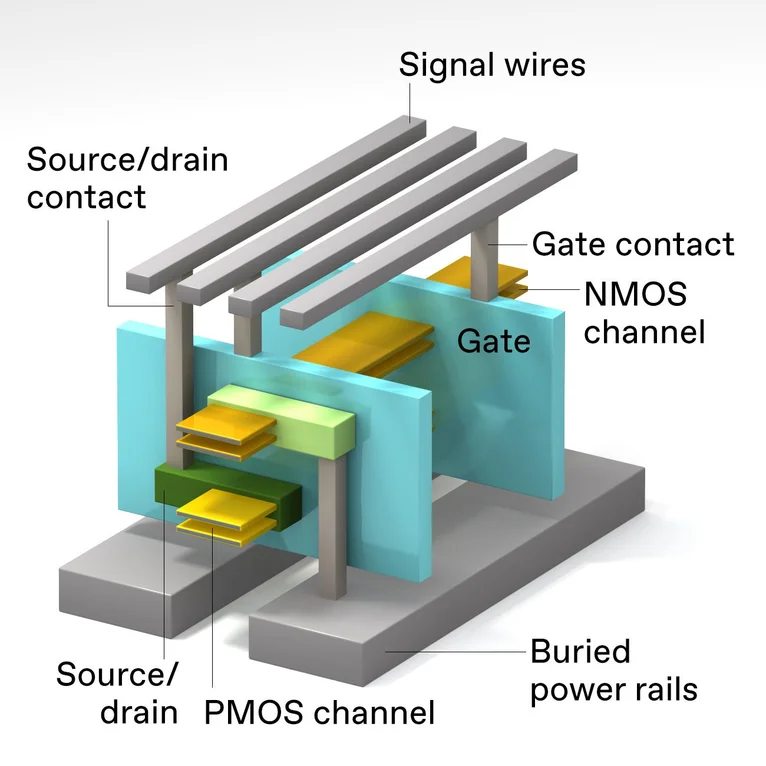
Making all the needed connections to 3D stacked CMOS is a challenge for Intel. Power connections will need to be made from below the device stack. In this design, the NMOS device [top] and PMOS device [bottom] have separate source/drain contacts, but both devices have a gate in common.EMILY COOPER
Image Credits: IEEE Spctrum
Read More: What are Intel Revenue Streams: Unraveling the 6 Pillars of Tech Giant
Intel 3D CMOS Vertical Stacking of CFET:
Intel’s research introduces a novel approach to transistor design by vertically stacking CFETs. This means that multiple CFETs are arranged on top of each other, creating a three-dimensional (3D) structure.
Gate Pitch Scaling to 60 Nanometers:
The gate pitch refers to the distance between the centers of two adjacent transistors on a semiconductor device. Intel’s breakthrough involves achieving a scaled gate pitch down to 60 nanometers. This indicates that the company has successfully reduced the spacing between transistors, allowing for a higher density of transistors within a given area.
Benefits of Stacking Transistors:
Stacking transistors vertically offers several advantages. One significant benefit is improved area efficiency. By utilizing the vertical space, Intel can pack more transistors into a smaller footprint.
Performance Enhancement:
The vertical stacking of CFETs also brings performance benefits. With transistors stacked on top of each other, there is a more efficient flow of electrical signals, reducing delays and improving overall performance. This is particularly important for achieving higher speeds and processing capabilities in electronic devices.
Beyond RibbonFET Technology:
Intel’s innovation in vertical stacking goes beyond the existing RibbonFET technology. RibbonFET is a type of gate-all-around (GAA) transistor architecture, and Intel’s latest research builds upon this foundation. GAA transistors offer improved electrostatic control over the channel, contributing to enhanced performance and energy efficiency.
Leadership in Gate-All-Around Transistors:
The use of gate-all-around transistors is a key aspect of Intel’s strategy. Gate-all-around transistors provide better control over the flow of electric current compared to traditional FinFET transistors. By achieving vertical stacking with CFETs, Intel solidifies its leadership in gate-all-around transistor technology.
Competitive Positioning:
The successful demonstration of vertically stacked CFETs at a scaled gate pitch positions Intel ahead of its competitors. This technological advancement showcases Intel’s capability to innovate in transistor design and reinforces its leadership in semiconductor technology.
Read More: Intel Most Advanced Process 18A to Enter Test Production by Early 2024
Conclusion:
Intel’s showcase at IEDM 2023 underscores its commitment to innovation and leadership in semiconductor technology. These breakthroughs secure the future of Moore’s Law and establish Intel as a pioneer in meeting evolving computing demands.