In a significant development in the electronics manufacturing landscape, Mumbai-based integrated electronics manufacturer Kaynes Technology is gearing up to establish a cutting-edge semiconductor OSAT (outsourced semiconductor assembly and test) manufacturing and compound semiconductor facility in Telangana. The project is set to be a game-changer, positioning Kaynes Technology as a prominent player in the semiconductor industry.
A Strategic Investment of Rs 2,800 Crore
Kaynes Technology is making a substantial investment of Rs 2,800 crore for the development of this advanced facility. Spanning across a sprawling 40-acre land in Ranga Reddy district, Telangana, the facility is poised to be a hub of innovation and progress. This strategic move underscores Kaynes Technology’s commitment to advancing its presence and capabilities in the semiconductor domain.
Read More: What is the Progress of Semiconductor Ecosystem in India in Last 2 years?
The Birth of Kaynes Semicon
Kaynes Technology is embarking on this ambitious venture through the establishment of Kaynes Semicon, a subsidiary crafted with the specific purpose of venturing into the OSAT/ATMP (assembly, testing, marking, and packaging) services sector. Kaynes Semicon aims to carve a distinctive niche within the highly competitive semiconductor industry by offering top-notch services and solutions.
Read More: First Indian Chipmaker to Go Public: Polymatech
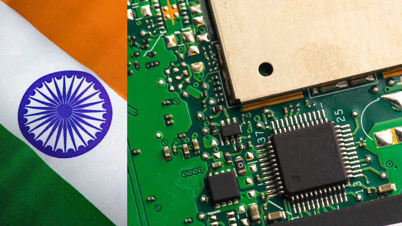
What is OSAT facility
OSAT stands for Outsourced Semiconductor Assembly and Test. It is a third-party service that suppliers around the world offer, which consists, as the name implies, of semiconductor assembly, packaging and testing of ICs (Integrated Circuits).
OSAT facilities play a vital role in the semiconductor industry. They provide a wide range of services to semiconductor companies, including:
- Wafer sawing and dicing
- Die bonding
- Wire bonding
- Encapsulation
- Testing
OSAT facilities are important because they allow semiconductor companies to focus on their core business of designing and manufacturing chips. By outsourcing assembly and testing to OSAT facilities, semiconductor companies can reduce costs, improve quality, and accelerate time to market.
Here are some of the benefits of using an OSAT facility:
- Reduced costs: OSAT facilities can help semiconductor companies reduce costs by providing high-quality services at a competitive price.
- Improved quality: OSAT facilities have the expertise and equipment to assemble and test chips to the highest quality standards.
- Accelerated time to market: OSAT facilities can help semiconductor companies accelerate time to market by providing quick turnaround times for assembly and testing services.
Overall, OSAT facilities are an important part of the semiconductor industry. They provide a wide range of services to semiconductor companies, which helps them to reduce costs, improve quality, and accelerate time to market.
Read More: 10 Hours to Learn Chip Packaging for Free
Job Creation and Economic Growth
Beyond technological advancements, this initiative is expected to make a significant socio-economic impact by creating over 2,000 direct jobs. These employment opportunities will not only contribute to local economic growth but also enhance skill development and empower the workforce. The infusion of talent and expertise will foster a culture of innovation and excellence within the semiconductor sector.
A Paradigm-Defining R&D Center
In a bid to amplify its technological capabilities, Kaynes Semicon will establish a dedicated Research and Development center focused on package research. Collaborating with the prestigious Indian Institute of Technology (IIT) Bombay, this center will drive innovation and research in semiconductor packaging. The partnership with IIT Bombay highlights Kaynes Semicon’s dedication to fostering academia-industry collaborations for mutual growth and development.
Enthusiastic Government Support
Telangana Industries & IT Minister, KT Rama Rao, officially announced and acknowledged Kaynes Technology’s OSAT venture. His endorsement further signifies the strategic alignment between the government’s vision and Kaynes Technology’s commitment to bolstering the semiconductor industry. The government’s support is instrumental in creating an enabling environment for businesses to thrive and innovate.
In conclusion, Kaynes Technology’s investment in the semiconductor industry with the establishment of the OSAT facility and compound semiconductor manufacturing in Telangana is a testament to the company’s vision, ambition, and dedication to technological excellence. This venture will undoubtedly play a pivotal role in shaping the future of the semiconductor landscape in India, paving the way for advancements, job creation, and economic growth.