Introduction
In the relentless pursuit of miniaturization and enhanced performance in the realm of electronics, a groundbreaking technology has emerged: 3D integrated circuits (3D ICs). These revolutionary chips transcend the conventional two-dimensional (2D) layout by stacking multiple layers of transistors and interconnects vertically, opening up a new dimension for circuit design and performance.
Read More: Explained: What the hell is a semiconductor? – techovedas
What is 3D ICs?
A 3D integrated circuit (3D IC) is a MOS (metal-oxide semiconductor) integrated circuit (IC) manufactured by stacking as many as 16 or more ICs and interconnecting them vertically using, for instance, through-silicon vias (TSVs) or Cu-Cu connections, so that they behave as a single device to achieve performance improvements at reduced power and smaller footprint than conventional two dimensional processes.
3D ICs promise “more than Moore” integration by packing improved functionality into small form factors while enhancing performance and reducing costs.
Evolution of 3D ICs
The Early Years of 3D ICs (1960s-1980s)
The concept of 3D ICs emerged in the 1960s, with researchers exploring various techniques for stacking multiple layers of transistors. However, the fabrication of 3D ICs was challenging due to the limitations of the technology at the time.
In the 1970s, researchers began to develop techniques for interconnecting multiple layers of transistors vertically. These techniques included through-silicon vias (TSVs) and wafer-to-wafer bonding.
The Rise of 3D ICs (1990s-2000s)
In the 1990s, 3D ICs began to gain traction as a viable technology for mainstream applications.However, This was due in part to advancements in fabrication techniques, which made it possible to manufacture 3D ICs with higher yields and lower costs.
The early 2000s saw the first commercial applications of 3D ICs. These applications were primarily in the areas of high-performance computing (HPC) and memory.
The Maturation of 3D ICs (2010s-Present)
In the 2010s, 3D ICs continued to mature and gain wider adoption. This was driven by the increasing demand for smaller, faster, and more energy-efficient electronic devices.
Today, 3D ICs are used in a wide range of applications, including HPC, mobile devices, artificial intelligence (AI), and aerospace and defense.
Read More: 15 Top Semiconductor companies in the World – techovedas
Real-Life Applications of 3D ICs:
3D ICs are poised to transform a wide range of electronic devices and applications, including:
High-Performance Computing (HPC):
3D ICs enable significant improvements in bandwidth and reduced latency, making them ideal for building powerful supercomputers and high-performance data processing systems. For instance, Intel’s Xeon Phi processor utilizes 3D IC technology to achieve significant performance gains in high-performance computing applications.
Example: The supercomputer Fugaku, powered by Fujitsu’s A64FX Arm processor, employs 3D IC technology to achieve a remarkable computing speed of 442 petaflops, making it the world’s fastest supercomputer.
Mobile Devices:
3D ICs can significantly enhance the performance and energy efficiency of mobile devices by enabling smaller form factors, increased transistor density, and reduced power consumption. Additionally,Samsung’s Exynos 2100 mobile processor employs 3D packaging to enhance performance and energy efficiency in smartphones.
Example: The Samsung Galaxy S22 Ultra, powered by the Exynos 2200 processor with 3D packaging, offers enhanced performance and battery life for demanding mobile applications.
Artificial Intelligence (AI) and Machine Learning (ML):
3D ICs can accelerate the development of AI and ML algorithms by providing the computational power and memory bandwidth required for complex AI applications. Cerebras Systems’ Wafer-Scale Engine, the world’s largest AI chip, utilizes 3D IC technology to achieve unprecedented AI processing power.
Example: OpenAI’s GPT-3 language model, powered by Cerebras Systems’ Wafer-Scale Engine, is capable of generating human-quality text, translating languages, and writing different kinds of creative content.
Aerospace and Defense:
3D ICs can enhance the capabilities of aerospace and defense systems by enabling smaller, lighter, and more powerful electronics for applications like radar, communication, and avionics. For instance, Raytheon Technologies is developing 3D ICs for radar systems that can detect and track targets with greater precision and range.
Example: Lockheed Martin’s F-35 Lightning II fighter jet utilizes 3D ICs in its electronic warfare systems to enhance situational awareness and electronic countermeasures capabilities.
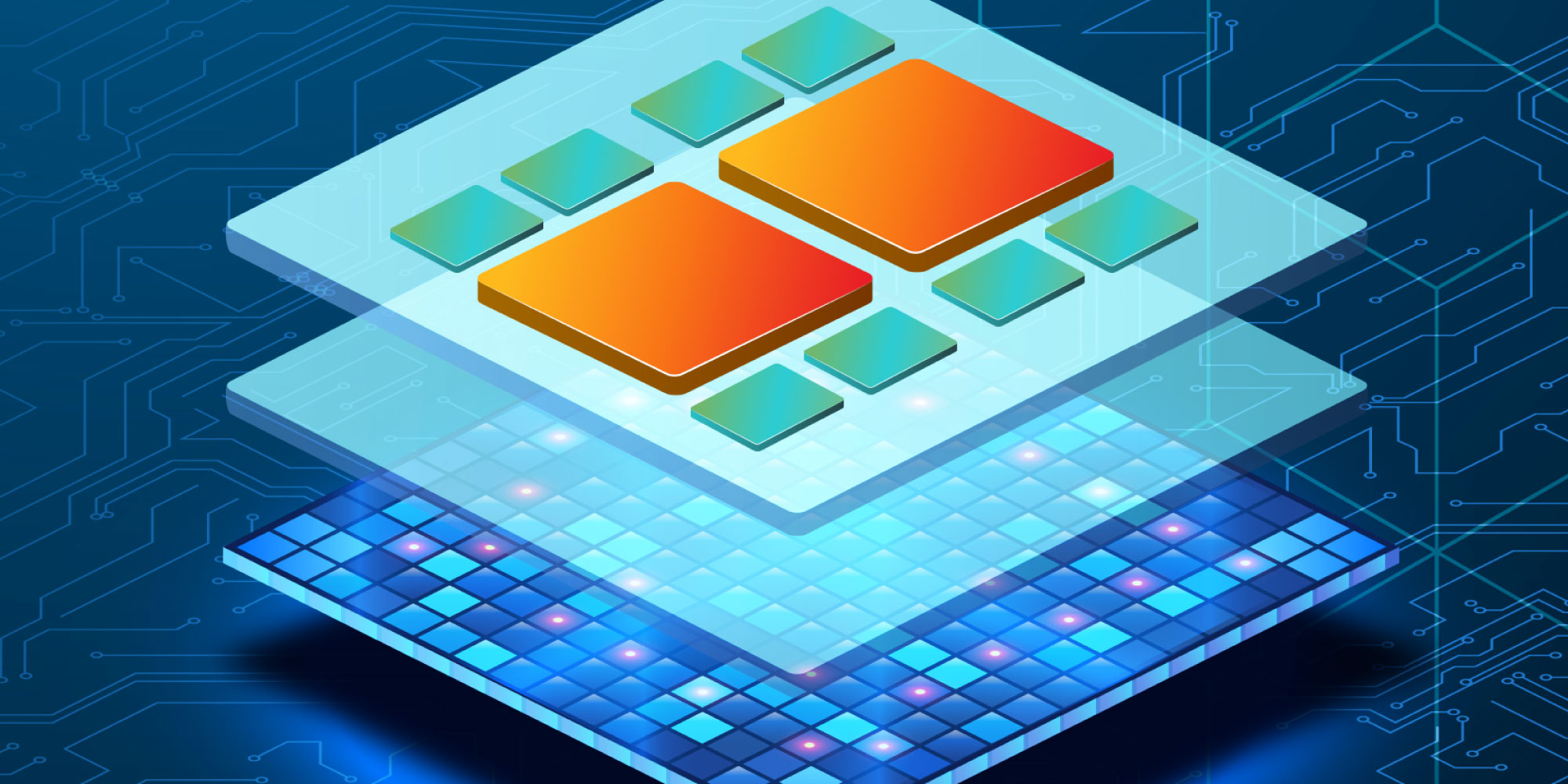
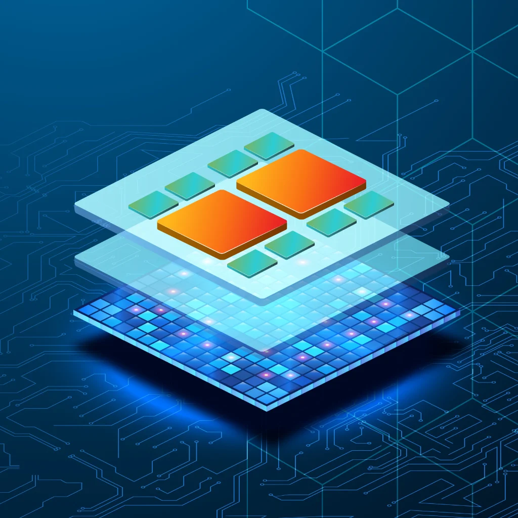
Working Principles of 3D ICs
The revolutionary concept of 3D ICs lies in the vertical stacking of multiple layers of transistors and interconnects, interconnected through various techniques such as through-silicon vias (TSVs) and wafer-to-wafer bonding. This vertical architecture offers several advantages over traditional 2D ICs:
Increased Transistor Density: 3D ICs can pack more transistors into a smaller area, leading to significant improvements in performance and power efficiency. This is achieved by stacking multiple layers of transistors vertically, significantly increasing the transistor count per unit area compared to traditional 2D ICs.
Reduced Interconnect Length: Shorter interconnects between transistors result in reduced signal propagation delays and improved signal integrity. Furthermore, In 3D ICs, interconnects between stacked layers are typically shorter than those in 2D ICs, leading to faster signal transmission and reduced latency.
Enhanced Bandwidth and Reduced Latency: 3D ICs enable efficient data transfer between stacked layers, providing higher bandwidth and reduced latency for demanding applications. Moreover, This is achieved through vertical interconnects that provide direct data paths between stacked layers, reducing the need for long horizontal interconnects that can introduce delays and signal integrity issues.
Importance of 3D ICs.
The advent of 3D Integrated Circuits (3D ICs) marks a pivotal moment in electronic design, offering solutions that transcend the limitations of traditional 2D ICs. Additionally,The importance of 3D ICs lies in their transformative impact on the electronic landscape, addressing key challenges and ushering in a new era of innovation.
Overcoming Scaling Limitations:
The significance of 3D ICs becomes apparent as they provide a practical solution to overcome these scaling limitations. By vertically stacking multiple layers of transistors and interconnects, 3D ICs enable increased transistor density without succumbing to the constraints of planar layouts, extending the trajectory of Moore’s Law.
Enhanced Performance and Efficiency:
The importance of 3D ICs is paramount as they revolutionize electronic performance. By efficiently packing more transistors into a smaller area and strategically reducing interconnect lengths, 3D ICs deliver a paradigm shift in performance and power efficiency.Moreover, The result is a notable technological leap forward, effectively addressing the shortcomings of their 2D counterparts.
Innovation in High-Performance Computing:
In the realm of high-performance computing, the need for increased bandwidth and reduced latency is paramount. However, traditional architectures face challenges in meeting these demands. Enter 3D ICs, which play a pivotal role in HPC by providing the necessary tools for unprecedented data processing capabilities. Notably, supercomputers and data processing systems leverage the vertical integration offered by 3D ICs, driving innovation in computational power and setting new standards in high-performance computing.
Energy Efficiency in Mobile Devices:
The energy efficiency and form factor limitations of mobile devices pose challenges that traditional 2D ICs struggle to address. 3D ICs emerge as a savior in this arena, significantly enhancing performance while enabling smaller form factors and reducing power consumption. This not only improves the user experience in smartphones and portable gadgets but also extends the battery life, marking a substantial leap in energy efficiency.
Acceleration of Artificial Intelligence (AI):
The computational demands of AI and machine learning algorithms necessitate specialized hardware architectures with high processing power and memory bandwidth. Additionally, this context, 3D ICs emerge as accelerators in the AI revolution, providing the computational power and memory bandwidth required for complex applications. Moreover, the increased transistor density and efficient vertical stacking of 3D ICs contribute to the rapid advancement of AI technologies.
Addressing Moore’s Law Extension:
Moore’s Law, a guiding principle predicting the exponential growth of transistor count and performance, faces challenges with traditional 2D IC designs. However, 3D ICs offer a tangible pathway to extend Moore’s Law beyond the constraints of their planar counterparts. Through vertical integration, 3D ICs continue to drive advancements in transistor density and performance. Consequently, they ensure that the trajectory set by Moore’s Law remains relevant in the evolving landscape of electronics.
In essence, the importance of 3D ICs is multifaceted. They represent a solution to scaling challenges, a catalyst for enhanced performance and efficiency, a versatile technology across applications, an innovator in high-performance computing, a game-changer in mobile device energy efficiency, a driving force in AI acceleration, and a key player in extending the legacy of Moore’s Law. As the electronic industry continues to evolve, 3D ICs stand as a cornerstone of progress, shaping a future where electronic systems are more powerful, efficient, and versatile than ever before.
Future Challenges Of 3D ICs
The evolution of 3D Integrated Circuits (3D ICs) has opened up new possibilities in electronic design, but it also presents several challenges that need to be addressed for widespread adoption and continued advancements. Here are five future challenges facing 3D IC technology:
Thermal Management:
As the transistor density increases in 3D ICs, efficient heat dissipation becomes a critical challenge. Moreover, the stacked layers of transistors generate more heat, and traditional cooling methods may become insufficient. Additionally, developing effective thermal management solutions to ensure that the temperature remains within acceptable limits is crucial for the reliability and longevity of 3D ICs.
Manufacturing Complexity:
The fabrication of 3D ICs involves intricate manufacturing processes, including precise stacking of multiple layers, through-silicon via (TSV) formation, and wafer bonding. Furthermore, as 3D ICs move from niche applications to mass production, streamlining and optimizing these complex manufacturing processes become imperative. Additionally, enhancements in fabrication techniques will be essential for cost-effective and scalable production.
Design Challenges:
Designing 3D ICs introduces new complexities compared to traditional 2D ICs. The vertical integration of multiple layers requires advanced design tools and methodologies. Ensuring signal integrity, managing power distribution, and optimizing the overall system design in three dimensions pose challenges for designers. The industry needs to develop and refine design tools that can efficiently handle the intricacies of 3D circuit design.
Standardization and Interoperability:
With the growing adoption of 3D ICs, there is a need for standardization in design rules, interfaces, and manufacturing processes. Standardization is crucial for ensuring interoperability between different components and systems from various manufacturers. Establishing industry-wide standards will facilitate collaboration, compatibility, and the development of a robust ecosystem around 3D IC technology.
Cost Considerations:
While 3D ICs offer numerous advantages, the initial costs associated with the technology can be higher than traditional 2D ICs. The intricate manufacturing processes, additional materials, and complexity in design contribute to increased production costs. To drive widespread adoption, there is a need to address these cost considerations, making 3D ICs more economically viable for a broader range of applications.
Addressing these challenges will require collaborative efforts from researchers, engineers, and industry stakeholders.
Follow us on LinkedIn for everything around Semiconductors & AI
Conclusion
3D Integrated Circuits (3D ICs) represent a transformative leap in electronic design, offering enhanced performance and miniaturization. Moreover, overcoming challenges like thermal management, manufacturing complexity, and standardization is vital for their widespread adoption. Consequently, as research progresses, 3D ICs are poised to revolutionize diverse industries, shaping the future of electronics.