Introduction:
In the ever-evolving world of technology, semiconductor Tech nodes & their applications play a pivotal role in shaping the capabilities of electronic devices.
The semiconductor nodes, measured in nanometers (nm), determine the size and efficiency of transistors on a chip, influencing the performance, power consumption, and overall functionality of electronic components.
In this blog post, we’ll explore specific applications across various semiconductor nodes, highlighting the cutting-edge devices and innovations that drive our digital world.
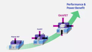
What is a Tech node?
Semiconductor technology nodes, often simply referred to as “nodes,” are a measurement of the manufacturing process used to produce semiconductor devices, like integrated circuits (ICs) or microchips.
The term “technology node” is essentially a shorthand way of describing the size of the individual transistors on a chip, and it is typically expressed in nanometers (nm).
The Pinnacle: Applications of Sub-7 nm Semiconductor Tech Nodes
1. Smartphones: Apple A16 Bionic Chip
The race to smaller nodes has led to the development of powerful mobile processors like the Apple A16 Bionic chip.
Built on a sub-7 nm process, this chip powers the latest generation of iPhones, providing unparalleled performance and energy efficiency. The smaller node allows for more transistors on the chip, enabling faster processing and improved power management.
2. AI Chips: Google Tensor Chip, Nvidia A100 GPU
Artificial Intelligence (AI) thrives on the processing power offered by sub-7 nm nodes. Google’s Tensor chip and Nvidia’s A100 GPU are prime examples.
These chips excel in machine learning tasks, utilizing the advanced transistor density to accelerate AI computations. From natural language processing to image recognition, these chips redefine the possibilities of AI applications.
3. High-Performance Computing (HPC) Chips: AMD Instinct MI300 Accelerator
HPC demands extreme processing capabilities, and the AMD Instinct MI300 accelerator delivers just that. With a sub-7 nm architecture, this chip targets scientific simulations, weather forecasting, and complex data analysis.
The smaller node allows for densely packed transistors, resulting in superior parallel processing performance.
Applications of 7-14 nm Semiconductor Tech Nodes
1. Memory Chips: Samsung 16Gb LPDDR5 DRAM
Moving into the 7-14 nm range, memory chips benefit from a balance between performance and power efficiency.
Samsung’s 16Gb LPDDR5 DRAM exemplifies this, offering high data transfer rates with relatively lower power consumption. This memory is crucial for supporting the increasing demands of modern applications and multitasking on devices.
2. GPUs: Nvidia GeForce RTX 3080 Ti
Gaming and graphics-intensive applications thrive on the processing power of GPUs. The Nvidia GeForce RTX 3080 Ti, built on a 7-14 nm node, delivers stunning graphics and real-time ray tracing. This node size strikes a balance, enabling a high number of transistors for graphical processing without compromising power efficiency.
3. Automotive Chips: NXP S32G390 Automotive Processor
In the automotive industry, chips must meet stringent reliability and performance requirements. The NXP S32G390 automotive processor, manufactured on a 7-14 nm node, integrates processing power with advanced safety features. This chip facilitates the development of autonomous driving and in-car connectivity.
Read More: How Chiplets Can Change the Future by extending Moore’s law
Applications of 14-28 nm Semiconductor Tech Nodes
1. Microcontrollers: STMicroelectronics STM32F767ZI
Microcontrollers form the backbone of embedded systems, and the STM32F767ZI from STMicroelectronics is a standout example. With a 14-28 nm node, this microcontroller strikes a balance between complexity and efficiency, making it ideal for a wide range of applications, from consumer electronics to industrial automation.
2. FPGAs: Xilinx Kintex UltraScale+
Field-Programmable Gate Arrays (FPGAs) offer flexibility in hardware design. The Xilinx Kintex UltraScale+, built on a 14-28 nm node, caters to diverse applications such as data center acceleration, communications, and aerospace. The larger node size allows for a good balance between configurability and performance.
3. ASICs: Bitcoin ASICs
Application-Specific Integrated Circuits (ASICs) are tailored for specific tasks, and Bitcoin mining is a classic example. ASICs designed for Bitcoin mining often operate on nodes in the 14-28 nm range, striking a balance between computational power and manufacturing cost.
4. Sensors: Bosch BMA460 Accelerometer
Sensors, crucial for various applications, also find their place in the 14-28 nm range. The Bosch BMA460 accelerometer, manufactured on this node, offers precision in measuring motion and tilt. This level of precision is essential in applications ranging from fitness trackers to industrial equipment.
5. Low-Cost Smartphones: MediaTek Helio G99
Low-cost smartphones aim to provide a balance between performance and affordability. The MediaTek Helio G99, with a 14-28 nm node, caters to this market segment by offering reliable performance for everyday tasks without the high manufacturing costs associated with smaller nodes.
Read more: Microprocessors vs. Microcontrollers: A Cake Analogy
Applications of 14-28 nm & above Semiconductor Tech Nodes
1. Power Management Chips: Texas Instruments TPS65218
Power efficiency is a critical consideration in electronic devices, and power management chips are key in achieving this. The Texas Instruments TPS65218, built on a 28 nm or larger node, provides efficient power management for a variety of devices, optimizing energy usage and extending battery life.
2. Display Drivers: Siliconix Si9136
Driving the displays of modern devices requires specialized components. The Siliconix Si9136 display driver, manufactured on nodes of 28 nm and above, ensures smooth and vibrant visuals across a range of devices, from smartphones to large-screen TVs.
3. Other Devices: Smart TVs, IoT Devices, Wearable Devices
Semiconductor nodes of 28 nm and above find application in a plethora of devices, including Smart TVs, Internet of Things (IoT) devices, and wearable devices. These nodes provide a cost-effective solution for devices where the absolute cutting-edge performance of smaller nodes may not be necessary.
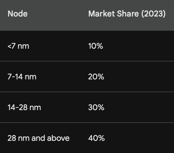
| Semiconductor Node | Applications and Examples |
|---|---|
| Sub-7 nm | – Smartphones: Apple A16 Bionic chip – AI Chips: Google Tensor chip, Nvidia A100 GPU – HPC Chips: AMD Instinct MI300 accelerator |
| 7-14 nm | – Memory Chips: Samsung 16Gb LPDDR5 DRAM – GPUs: Nvidia GeForce RTX 3080 Ti – Automotive Chips: NXP S32G390 automotive processor |
| 14-28 nm | – Microcontrollers: STMicroelectronics STM32F767ZI – FPGAs: Xilinx Kintex UltraScale+ FPGA – ASICs: Bitcoin ASICs – Sensors: Bosch BMA460 accelerometer – Low-Cost Smartphones: MediaTek Helio G99 |
| 28 nm and above | – Power Management Chips: Texas Instruments TPS65218 – Display Drivers: Siliconix Si9136 – Other Devices: Smart TVs, IoT devices, wearable devices |
Read More: 5 Major hurdles in Chiplet Adoption as More than Moore Solution?
Conclusion:
As semiconductor technology continues to advance, the diverse range of applications across different nodes showcases the versatility of these tiny but powerful components. From the pocket-sized smartphones to the massive computational power of HPC chips, each node size brings its own set of advantages, catering to the specific needs of various industries and applications. The semiconductor landscape is a testament to the relentless pursuit of innovation, shaping the way we interact with technology in our daily lives.