
Introduction:
In the intricate world of semiconductor manufacturing, where precision and control are paramount, Rapid Thermal Annealing (RTA) emerges as a pivotal process, exerting a profound impact on the properties of semiconductor materials.
This blog post delves into the nuances of RTA, exploring its significance, underlying mechanisms, applications, and the transformative influence it wields in the quest for ever-smaller, faster, and more efficient electronic devices.
Follow us on Linkedin for everything around Semiconductors & AI
Understanding Rapid Thermal Annealing:
RTA is a semiconductor processing technique designed to enhance the crystalline structure of materials through short, intense bursts of heat. Unlike traditional furnace annealing, RTA’s hallmark lies in its swift heating and cooling cycles, typically within seconds. This rapidity prevents the diffusion of atoms to undesired locations, allowing for precise control over material properties.
Mechanisms at Play:
The crux of RTA lies in the intricate interplay of thermal energy with semiconductor materials. As the material is rapidly heated to elevated temperatures (often in the range of 1,000 to 1,200 degrees Celsius), several crucial processes unfold:
- Activation of Dopants: RTA facilitates the activation of dopants, introducing specific impurities into the semiconductor material to modulate its electrical properties. This is crucial for tailoring conductivity and achieving desired electronic characteristics.
- Crystallization Enhancement: Rapid heating and cooling cycles prevent the formation of amorphous regions, promoting the growth of a highly crystalline structure. This has profound implications for the performance of semiconductor devices.
- Annealing of Defects: Defects and imperfections in the crystal lattice, arising from prior manufacturing steps, are rectified during RTA. The process aids in the elimination of defects, contributing to improved material quality.
Read More : What is Quantum Entanglement; Applications and Challenges – techovedas
Applications Across Semiconductor Technologies:
- CMOS Fabrication: RTA finds widespread application in Complementary Metal-Oxide-Semiconductor (CMOS) technology. It plays a key role in activating dopants in the source and drain regions, influencing the overall performance of transistors.
- Memory Devices: In the production of memory devices, RTA is employed for crystallization of thin films, enhancing the performance of non-volatile memory technologies such as Flash and Phase Change Memory (PCM).
- Optoelectronics: RTA is integral in the fabrication of optoelectronic devices, influencing the properties of materials used in light-emitting diodes (LEDs), laser diodes, and photodetectors.
- Advanced Semiconductor Nodes: As semiconductor technology advances towards smaller nodes, RTA becomes increasingly critical. It allows for precise control in the formation of ultra-shallow junctions and the activation of dopants in nanoscale devices.
Read More: Explained: What is FPGA – techovedas
How do they work?
Rapid Thermal Annealing (RTA) is a semiconductor manufacturing process that involves quickly heating and cooling semiconductor materials to modify their properties. The process is crucial for tailoring the electrical and structural characteristics of semiconductor devices. Here’s a breakdown of how RTA works:
1. Swift Heating:
- RTA involves exposing the semiconductor material to a rapid and intense burst of heat, typically within seconds.
- The heating is achieved using high-intensity lamps or other energy sources that can quickly elevate the temperature of the material.
2. Controlled Temperature:
- The material is heated to specific temperatures, often ranging from 1,000 to 1,200 degrees Celsius.
- The temperatures and duration of heating are carefully controlled to achieve precise modifications in the material’s properties.
3. Activation of Dopants:
- One of the primary purposes of RTA is to activate dopants within the semiconductor material.
- Dopants are specific impurities intentionally introduced into the material to alter its electrical properties. The rapid heating activates these dopants, allowing them to contribute to the desired conductivity characteristics.
4. Crystallization Enhancement:
- RTA promotes the growth of a highly crystalline structure within the semiconductor material.
- The rapid heating and cooling cycles prevent the formation of amorphous regions, ensuring that the material has a well-defined and ordered crystal lattice structure.
5. Annealing of Defects:
- Semiconductor materials often contain defects or imperfections in their crystal lattice due to prior manufacturing steps.
- RTA serves as an annealing process, helping to eliminate these defects and enhance the overall quality of the material.
Importance of Rapid Thermal Annealing
In the dynamic realm of semiconductor manufacturing, Rapid Thermal Annealing (RTA) emerges as a pivotal process, wielding influence over the properties of materials crucial to electronic devices. This article delves into the importance of RTA and explores the challenges that pave the way for future innovations in semiconductor technology.
Precision in Doping Activation:
- RTA plays a fundamental role in activating dopants within semiconductor materials, ensuring precision in the creation of conductive regions essential for transistor functionality.
- This precision is particularly critical in advanced CMOS fabrication processes, where accurate doping profiles are imperative for transistor performance.
Enhancing Crystalline Structure:
- The ability of RTA to promote the growth of a well-defined crystalline structure is vital for semiconductor materials.
- Enhanced crystallinity contributes to improved carrier mobility and overall electrical performance in electronic devices.
Memory Device Advancements:
- RTA is a linchpin in the production of memory devices, facilitating the crystallization of thin films crucial for the operation of non-volatile memory technologies like Flash and Phase Change Memory.
- This advancement is pivotal for the continual evolution of high-density and high-speed memory solutions.
Optoelectronic Device Fabrication:
- Optoelectronic devices, including LEDs, laser diodes, and photodetectors, benefit significantly from the precision and control offered by RTA.
- The process contributes to the creation of semiconductor materials with tailored optical and electrical properties.
Enabling Advanced Semiconductor Nodes:
- As semiconductor technologies advance to smaller nodes, RTA becomes indispensable for achieving the precise control needed for forming ultra-shallow junctions and activating dopants in nanoscale devices.
- It plays a crucial role in maintaining the integrity and performance of devices at these advanced nodes.
Difference between RTA and RTP
Semiconductor manufacturing is a realm of precision, and thermal processes play a pivotal role in shaping material properties. Two key techniques, Rapid Thermal Annealing (RTA) and Rapid Thermal Processing (RTP), are integral to this domain. Let’s delve into their nuances and understand how they differ.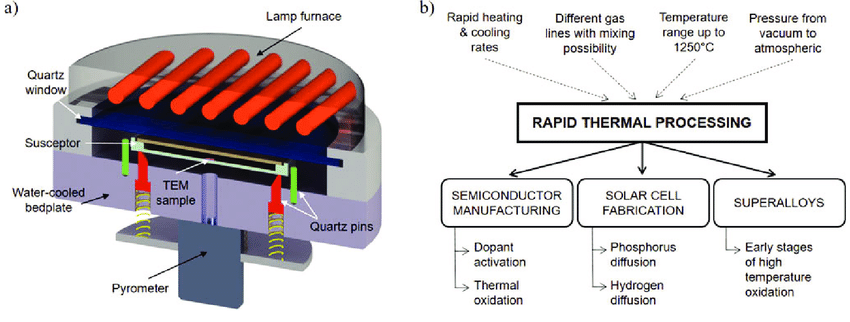
| Aspect | Rapid Thermal Annealing (RTA) | Rapid Thermal Processing (RTP) |
|---|---|---|
| Definition | Rapid heating and cooling for annealing semiconductor materials, focusing on improving crystallinity and dopant activation. | Broader term covering various rapid thermal processes, including annealing, oxidation, nitridation, and chemical vapor deposition. |
| Application | Predominantly used for annealing, especially in CMOS fabrication and memory device production. | Encompasses a wide range of thermal processes, addressing needs beyond annealing, such as oxidation and deposition. |
| Timeframe | Extremely short processing times (seconds to minutes) for quick heating and cooling cycles. | Varied timeframes depending on the specific process, with some being as rapid as RTA and others involving longer durations. |
| Control and Precision | Known for exceptional control and precision, achieving uniform heating and localized thermal treatment. | Provides flexibility in control and precision, with variations based on specific applications and thermal processes. |
This table summarizes the key differences between RTA and RTP, highlighting their distinct focuses, applications, timeframes, and levels of control.
In essence, while RTA is a specialized technique concentrating on rapid annealing for specific semiconductor applications, RTP is a versatile approach covering a broader set of rapid thermal processes used throughout semiconductor manufacturing stages. The distinction lies in the scope, application, and specificity of the thermal processes involved in each technique.
Future Challenges and Innovations:
Uniform Heating Across Wafers:
- Challenge: Ensuring uniform heating across large wafers poses a persistent challenge.
- Innovation: Ongoing research focuses on developing advanced heating technologies and methodologies to achieve uniform temperature profiles, enhancing the consistency of RTA processes.
Addressing Thermal Budget Constraints:
- Challenge: As devices become smaller, managing the thermal budget becomes increasingly challenging.
- Innovation: Researchers are exploring novel cooling techniques and optimizing thermal management strategies to meet stringent thermal constraints without compromising performance.
Reproducibility in Nanoscale Processes:
- Challenge: Achieving reproducibility in nanoscale processes is a key concern.
- Innovation: Advancements in process control technologies, machine learning applications, and in-situ monitoring techniques aim to enhance reproducibility and reduce variability in RTA processes.
In conclusion, Rapid Thermal Annealing stands at the forefront of semiconductor manufacturing, driving precision and control in the creation of electronic devices. While challenges persist, ongoing innovations hold the promise of overcoming these hurdles, shaping the future of semiconductor technology.
Conclusion:
Rapid Thermal Annealing stands as a testament to the meticulous dance of science and engineering in semiconductor manufacturing. Its ability to impart specific properties to materials with unprecedented precision underscores its indispensable role in the relentless pursuit of semiconductor advancements. As electronic devices continue to evolve, RTA will undoubtedly remain a linchpin in the ever-expanding toolkit of semiconductor engineers, shaping the very foundation of our connected world.