Introduction
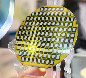
In the dynamic world of semiconductor manufacturing, Reactive Ion Etching (RIE) stands as a pivotal process, wielding precision and control in the etching of materials.
Let’s embark on a comprehensive journey to uncover the intricacies of RIE, exploring its real-life applications, underlying mechanisms, functions, recent advancements, challenges, and peering into the future possibilities it holds.
Follow us on LinkedIn for everything around Semiconductors & AI
Understanding Reactive Ion Etching (RIE):
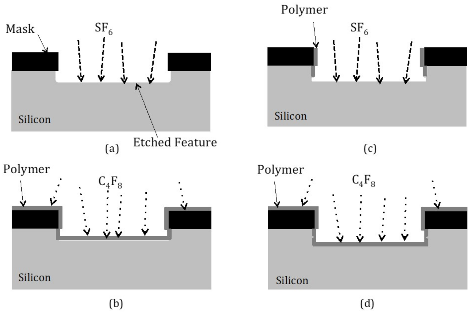
Imagine you have a piece of wood, and you want to carve a specific design into it. Instead of using a traditional carving tool like a chisel, you decide to use a laser beam. The laser, on its own, might not be very effective at cutting into the wood. However, if you introduce a reactive gas into the process, it becomes much more powerful.
In this analogy:
- The wood represents the material you want to etch (e.g., a silicon wafer in semiconductor manufacturing).
- The laser beam corresponds to the ionized particles used in the etching process.
- The reactive gas is the additional element that enhances the etching capabilities. It chemically reacts with the material, making the process more effective.
So, in Reactive Ion Etching, the combination of ionized particles and reactive gases is used to precisely etch patterns and structures onto materials for various applications in electronics and microfabrication.
Read More: Top 10 Semiconductor Companies of Europe by Market Cap in 2023 – techovedas
Types of Reactive Ion Etching
Reactive Ion Etching (RIE) can be categorized into different types based on various parameters such as pressure, power, and the type of reactive gases used. Here are some common types of RIE:
High-Density Plasma (HDP-RIE):
- Characteristics: Operates at high gas pressures and high plasma densities.
- Applications: Suitable for deep and anisotropic etching, often used in microelectromechanical systems (MEMS) and semiconductor device fabrication.
Inductively Coupled Plasma (ICP-RIE):
- Characteristics: Employs inductively coupled plasma to generate high-density reactive species.
- Applications: Offers higher ion density, making it suitable for high-aspect-ratio etching, deep silicon etching, and advanced semiconductor processes.
Cryogenic RIE:
- Characteristics: Operates at low temperatures, often using liquid nitrogen or other cryogenic gases.
- Applications: Useful for materials that tend to have high thermal sensitivity, such as certain polymers and biological materials.
Electron Cyclotron Resonance (ECR-RIE):
- Characteristics: Uses microwaves to create a high-density plasma in a magnetic field.
- Applications: Suitable for low-pressure etching and is often used for delicate materials where ion damage needs to be minimized.
Which RIE to use When
Choosing the appropriate type of RIE depends on the specific requirements of the material and the desired etching results. Here are some considerations:
- Material Type: Different materials have varying sensitivities to temperature and ion damage. Choose an RIE method that aligns with the material properties.
- Etch Selectivity: Consider the selectivity of the etching process. Some RIE methods may offer better selectivity for certain materials or layers.
- Aspect Ratio: For applications requiring high-aspect-ratio features, such as deep trench etching, high-density plasma or ICP-RIE might be preferred.
- Temperature Sensitivity: If the material is sensitive to temperature, cryogenic RIE may be suitable to minimize thermal damage.
- Precision and Uniformity: Depending on the application, the uniformity and precision of etching may be crucial, and specific RIE methods may offer better control in these aspects.
- Cost and Accessibility: The equipment and operational costs can vary between different RIE systems. Consider budget constraints and the availability of equipment.
In summary, the choice of RIE depends on the specific requirements of the material and the desired etching characteristics for a particular application. Researchers and engineers often need to balance factors such as etch rate, selectivity, and damage to achieve the desired results.
Functions of Reactive Ion Etching (RIE):
Anisotropic Material Removal:
In the ballet of material removal, RIE’s anisotropic dance takes center stage. Its function ensures etched structures stand tall with straight, well-defined sidewalls, contributing to the precision of the final masterpiece. This anisotropic nature is achieved by using reactive ions that predominantly remove material in the vertical direction, resulting in superior control over the shape of etched features.
Selective Etching:
RIE’s function of selective etching is akin to a painter delicately choosing colors. It targets specific materials, leaving others untouched, crucial in the controlled removal of materials during the fabrication process. The selectivity of RIE is achieved through the choice of reactive gases and process conditions, allowing for the tailored etching of specific materials while preserving others.
High Aspect Ratio Etching:
RIE’s ability to achieve high aspect ratios transforms etched features into towering sculptures. The function allows for the creation of three-dimensional structures with intricate details, defining the depth of the artistic creation. Achieving high aspect ratios is particularly valuable in advanced semiconductor manufacturing, where the demand for complex and compact structures is ever-present.
Material Compatibility:
RIE’s versatility is a testament to its material compatibility. It adapts to a diverse array of materials commonly used in semiconductor fabrication, showcasing its ability to paint on various canvases with finesse. The compatibility spans semiconductors, metals, and dielectrics, making it an indispensable tool in the semiconductor industry. The process can be customized for different materials, allowing for the creation of intricate multi-material structures.
Recent Advancements in RIE Technology:
Nanotechnology Integration:
As RIE ventures into the microscopic realm of nanotechnology, it eagerly embraces recent advancements. These cutting-edge developments contribute significantly to the creation of nanostructures with unprecedented precision. The canvas becomes infinitesimally small, and RIE’s strokes become finer. Consequently, in this meticulous pursuit, nanotechnology integration involves pushing the limits of resolution and precision to new frontiers. Consequently, this opens up exciting possibilities for applications in diverse fields like nanoelectronics and nanophotonics.
Plasma Process Optimization:
Within the laboratory of plasma processes, researchers refine RIE’s strokes. Ongoing research focuses on optimizing plasma processes to enhance uniformity and reduce side effects, contributing to improved etching quality. Plasma process optimization is crucial for achieving consistent and high-quality results across large semiconductor wafers, ensuring uniformity in etched features.
Challenges and Ongoing Research:
Mask Damage:
Even in the realm of precision, challenges persist. RIE’s delicate brushstroke sometimes leads to mask damage, and researchers work tirelessly to optimize processes, minimizing the impact on the final artwork. Mask damage can affect the fidelity of the patterns being etched, and ongoing research aims to develop protective strategies and alternative materials to mitigate this challenge.
Material Compatibility in Advanced Nodes:
Adapting RIE for novel materials in advanced semiconductor nodes is an artistic challenge. Researchers explore new chemistries and process optimizations to ensure compatibility with emerging materials, pushing the boundaries of its creative palette. Advanced semiconductor nodes often involve the use of new materials with unique properties, requiring RIE to evolve and adapt to these changing requirements.
Environmental Concerns:
Beyond the cleanroom, environmental concerns emerge. The chemicals used in RIE processes can raise ecological questions, prompting researchers to explore and implement eco-friendly alternatives, ensuring that the artistic process aligns with sustainability goals. Addressing environmental concerns involves developing greener processes without compromising the precision and efficiency of RIE.
Integration with Next-Generation Technologies:
As technology marches forward, RIE faces the challenge of integration with next-gen technologies, such as quantum computing and the use of 2D materials. Researchers are actively exploring ways to adapt and optimize RIE processes for these cutting-edge applications. Integration with next-generation technologies requires a deep understanding of the unique material properties and processing requirements, presenting both opportunities and challenges for RIE.
Conclusion:
Reactive Ion Etching stands at the forefront of semiconductor manufacturing, facilitating the creation of intricate structures that power our electronic devices. As we navigate through its functions, applications, recent advancements, challenges, and ongoing research, the future of RIE holds promises of even greater precision and innovation. With continuous exploration and advancements, Reactive Ion Etching continues to be a driving force in shaping the landscape of modern semiconductor technology. The artistry of RIE, with its precision and adaptability, paves the way for the next generation of semiconductor devices that will shape the digital landscape of tomorrow.