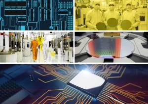
Introduction
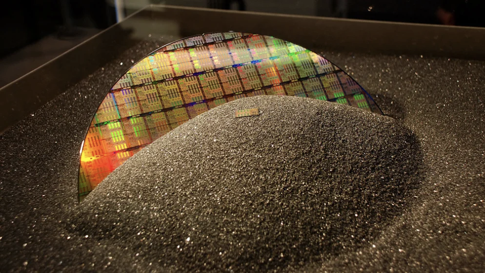
Imagine a thin slice of silicon, about the size of a pizza, that can power millions of devices, from smartphones to cars to solar panels. That’s what a silicon wafer is, and it’s the backbone of the semiconductor industry, which produces the electronic chips that enable the digital world.
But as the world becomes more connected, more intelligent, and more demanding, the semiconductor industry needs to keep up with the increasing demand for faster, cheaper, and better chips. And one of the ways to do that is to make the silicon wafers bigger.
Follow us on Linkedin for everything around Semiconductors & AI
What is a silicon wafer and why do they matter?
Silicon wafers are made from pure silicon, which is extracted from sand and melted into cylindrical blocks called ingots. These ingots are then cut into thin discs, polished, and processed to create the electronic circuits that run various devices.
The size of the wafers affects how many chips can be made in one batch, which influences the cost, quality, and performance of the final products. The bigger the wafer, the more chips can be squeezed onto it, and the lower the cost per chip.
Applications of Different sized Silicon Wafer
| Wafer Size | Technology Nodes | Applications | Cost Considerations |
|---|---|---|---|
| 2 inches | Older nodes | Early electronic devices | Lower cost due to smaller size and older tech |
| 3 inches | Older nodes | Basic electronic components | Lower cost, but slightly more expensive than 2″ |
| 4 inches | Older nodes | Simple integrated circuits | Economies of scale start to impact cost |
| 6 inches | Older to mid-range nodes | Microcontrollers, basic processors | Larger scale production, moderate cost reduction |
| 8 inches | Mid-range nodes | Processors, memory chips | Economies of scale, improved production efficiency |
| 12 inches | Mid-range to advanced nodes | Advanced processors, memory, SoCs | Significant cost reduction due to larger scale production |
| 300mm | Advanced nodes | High-performance processors, GPUs | Further cost reduction, increased chip yield |
It’s important to note that the correlation between wafer size and technology nodes isn’t always direct, as advancements in manufacturing processes can enable smaller nodes on larger wafers. Additionally, the cost is influenced by factors such as yield, production volume, and the complexity of the manufacturing process.
The evolution of technology nodes (e.g., 65nm, 45nm, 7nm) is indicative of the level of miniaturization and performance achievable on a chip. As technology nodes decrease in size, more transistors can be packed onto a chip, improving performance.
However, the cost of manufacturing at smaller nodes tends to increase due to the complexity and precision required in the manufacturing process.
Also Read: Why Silicon Wafers Are Round and Chips are Square?
How has silicon wafer grown over time?
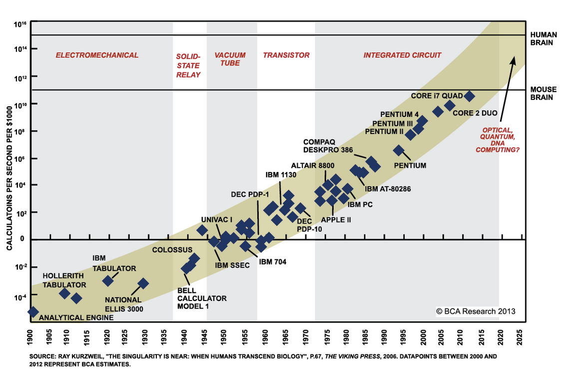
Silicon wafers have grown steadily over the decades, following the trend of Moore’s law, which predicts that the number of transistors on a chip doubles every two years.
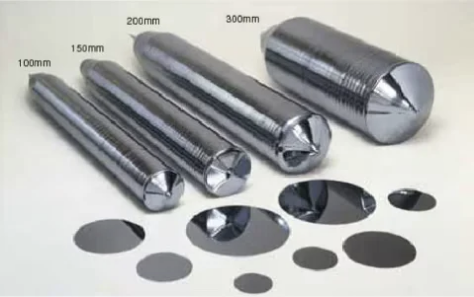
The first commercial silicon wafers in the 1950s were only 25 mm (1 inch) in diameter, and could fit only a few transistors. By the 1980s, the wafers reached 150 mm (6 inches), and could fit thousands of transistors.
In the 1990s, the wafers grew to 200 mm (8 inches), and could fit millions of transistors. In the 2000s, the wafers expanded to 300 mm (12 inches), and could fit billions of transistors.
The current standard wafer size is 300 mm, which can produce about 2.5 times more chips than a 200 mm wafer, and reduce the cost per chip by about 30%.

But as the semiconductor industry reaches the physical limits of shrinking the transistor size, the benefits of making the chips smaller are fading, and the challenges of maintaining quality and reliability are rising.
Therefore, the industry is looking for other ways to boost the chip performance and productivity, and one of them is making the wafers bigger.
The size of silicon wafers has evolved over the years to accommodate the increasing demand for smaller and more powerful electronic devices.
Wafer Size is correlated with Advancements in Technology
| Year | Technology/Methodology | Key Features/Advancements | Wafer Size |
|---|---|---|---|
| 1960s | Czochralski (Cz) method | Invention of the Czochralski method for crystal growth | 2 inches |
| 1970s | Silicon Epitaxy | Introduction of epitaxial growth for thin-film layers | 3 inches |
| 1980s | Float-Zone (FZ) method | Reduced impurities and improved crystal quality | 4 inches |
| 1990s | Silicon on Insulator (SOI) | Enhanced insulation properties for improved performance | 6 inches |
| 2000s | Advanced Czochralski techniques | Improved crystal uniformity and larger wafer sizes | 8 inches |
| 2010s | FinFET Transistors | Transition to 3D transistors for better performance | 12 inches |
| 2020s | Extreme Ultraviolet (EUV) Lithography | Advancement in lithography for smaller feature sizes | 300mm (approximately 12 inches) |
The semiconductor industry drives the transition to larger wafer sizes, like moving from 8 inches to 12 inches, to increase the number of chips produced per wafer, thereby improving efficiency and reducing manufacturing costs.
The industry standard for silicon wafers in recent years has been 300mm, or approximately 12 inches.
Also Read: How Larger Wafers Are Driving Innovation in the Chip Industry
What are the pros and cons of big Silicon wafer?
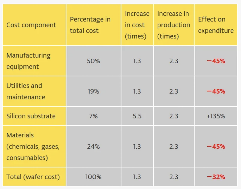
Production Cost Analysis by SEMATECH on 450mm vs 300mm wafers
Pros of Big Silicon Wafer:
Higher Efficiency in Manufacturing:
- In a single batch, larger wafers increase manufacturing efficiency by allowing the production of more semiconductor devices.
Cost Reduction:
- The use of larger wafers can lead to cost savings as it reduces material wastage and energy consumption per chip produced.
Increased Throughput:
- Larger wafers can accommodate more individual chips, leading to higher throughput during the semiconductor fabrication process.
Improved Yields:
- Larger wafers can potentially result in higher yields per wafer, reducing the impact of defects on the overall production.
Enhanced Productivity:
- With more chips produced simultaneously, there is an overall increase in productivity, meeting the growing demand for semiconductor devices.
Cons of Big Silicon Wafer:
Equipment Costs:
- Manufacturing equipment for processing larger wafers can be expensive, requiring significant capital investment for upgrading or building new fabrication facilities.
Technology Challenges:
- Adopting larger wafers may require advancements in technology to ensure uniformity, precision, and defect control during the manufacturing process.
Transition Period:
- Transitioning to larger wafers may involve a period of adjustment for manufacturers, leading to potential disruptions and increased costs during the transition.
Wafer Handling Issues:
- Larger wafers are more susceptible to handling issues, breakage, and contamination, which can impact the overall yield and quality of the semiconductor devices.
Limited Compatibility:
- The adoption of larger wafers may not be universally compatible with existing semiconductor fabrication technologies and infrastructure, requiring extensive modifications.
In summary, while big silicon wafers offer advantages in terms of efficiency and cost, their adoption comes with challenges related to equipment costs, technology readiness, and compatibility issues that need careful consideration by semiconductor manufacturers.
Read More: Which Country is the leader in Semiconductor Value chain?
450mm vs 300mm wafers
The semiconductor industry expects the next-generation wafer size to be 450 mm (18 inches), enabling the production of approximately 2.25 times more chips than a 300 mm wafer and reducing the cost per chip by about 30%. This can help the semiconductor industry meet the growing demand for chips in various applications, such as:
- Artificial Intelligence
- Cloud Computing
- 5G
- Internet of Things
- Autonomous Vehicles.
But making the wafers bigger is not easy. It requires,
- Huge investments in new equipment, facilities, materials, and technologies,
- Cooperation among different players, such as chip makers, equipment suppliers, material providers, and customers.
What is the current status and future outlook of big wafers?
The development of big wafers has been going on for several years, but the adoption has been slow and uncertain. The transition’s high cost and risk have deterred many chip makers and customers from investing in big wafers.
Moreover, the COVID-19 pandemic has disrupted the global supply chain and demand for semiconductors, creating further challenges and uncertainties for the industry.
However, some chip makers and equipment suppliers have continued to pursue big wafers, and have made some progress in recent years.
For example, Intel, one of the leading chip makers, has announced its plans to start producing chips on 450 mm wafers by 2025, and has invested in new facilities and equipment for big wafers.
ASML, one of the leading equipment suppliers, has delivered its first 450 mm lithography system to a customer in 2019, and has been working on improving its performance and reliability.
The future of big wafers depends on the balance between the pros and cons, as well as the collaboration and coordination among the industry players. If the industry can overcome the technical and economic hurdles, and achieve a consensus on the standards and timelines, big wafers can offer a significant advantage for the semiconductor industry in the long term.
Conclusion
Silicon wafers are the key material for the semiconductor industry, and their size has a significant impact on the cost, quality, and performance of the chips. The industry is facing the need and opportunity to scale up the wafer size from 300 mm to 450 mm, which can enable more chip production and lower cost per chip.
However, the transition to big wafers is also fraught with challenges and uncertainties, which require substantial investments and cooperation among the industry players.
The future of big wafers will depend on how the industry can overcome the obstacles and leverage the advantages of big wafers.