
Introduction:
In a significant milestone for the semiconductor industry, Samsung Electronics, in collaboration with Synopsys, has successfully taped out its first mobile system-on-chip (SoC) utilizing Samsung Foundry’s cutting-edge 3nm gate-all-around field-effect transistor (GAAFET) process technology.
This achievement marks a pivotal moment for Samsung as it enters the realm of advanced semiconductor manufacturing for smartphone application processors.
Samsung manufactured its first mobile system-on-chip (SoC) using a 3nm GAAFET process. This is a major milestone as it signifies Samsung’s progress in using this advanced chip manufacturing technique for smartphones and other complex devices.
GAAFET stands for Gate-All-Around Field-Effect Transistor. It’s a new transistor design that promises better performance and power efficiency compared to the previous FinFET technology used in 5nm and 7nm chips.
Samsung collaborated with Synopsys, a company specializing in electronic design automation (EDA) tools. Synopsys’ tools likely aided Samsung in designing and verifying the layout of the new 3nm GAAFET SoC.
Follow us on Linkedin for everything around Semiconductors & AI
Samsung Move to Advanced Semiconductor Manufacturing: GAAFET
While Samsung Foundry has been at the forefront of chip production using its GAAFET-equipped SF3E process for nearly two years, this announcement signals Samsung Electronics’ first foray into utilizing this technology for its own SoCs.
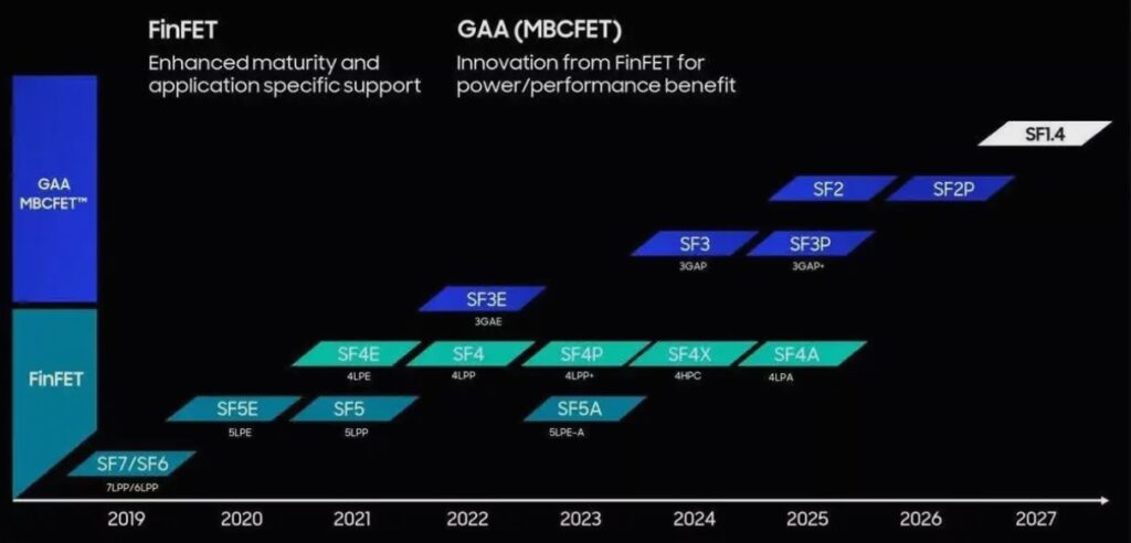
SF3E was mainly used for cryptocurrency mining chips initially. This was because of early teething issues and yield challenges in pioneering commercial GAAFET processes.
Collaboration with Synopsys with GAAFET
Samsung Electronics and Synopsys collaborated closely to develop the high-performance mobile SoC. Samsung utilized Synopsys’ advanced EDA suite, including tools like DSO.ai and Fusion Compiler RTL-to-GDSII solution, to optimize design, maximize yields, and boost performance.
“Our longstanding collaboration has delivered leading-edge SoC designs. This is a remarkable milestone to successfully achieve the highest performance, power and area on the most advanced mobile CPU cores and SoC designs in collaboration with Synopsys. Not only have we demonstrated that AI-driven solutions can help us achieve PPA targets for even the most advanced GAA process technologies, but through our partnership we have established an ultra-high-productivity design system that is consistently delivering impressive results.”
~Kijoon Hong, vice president of SLSI at Samsung Electronics. “
Key Achievements and Improvements for Samsung GAAFET:
The collaborative efforts between Samsung and Synopsys yielded remarkable enhancements in the SoC’s performance, power efficiency, and area utilization. Notably, the chip’s peak clock speed was boosted by 300MHz while reducing dynamic power usage by 10%.
This feat was accomplished through innovative design partitioning optimization, multi-source clock tree synthesis (MSCTS), and smart wire optimization techniques. These methods were aided by a simplified hierarchical approach.
Performance (300MHz clock speed boost):
- Innovative design partitioning optimization: This could involve dividing the chip into smaller, more efficient blocks that can communicate effectively. This reduces signal travel distances and minimizes delays, allowing for higher clock speeds.
- Multi-source clock tree synthesis (MSCTS): Traditionally, a single clock source feeds the entire chip. Here, MSCTS might distribute the clock signal from multiple points, ensuring it reaches all parts of the chip at the same time. This avoids clock skew (timing variations) and enables higher operating frequencies.
Power Efficiency (10% dynamic power reduction):
- Smart wire optimization techniques: This likely involves optimizing the layout of wires within the chip. Thinner wires use less power, but can’t carry as much current. Thicker wires carry more current but consume more power. Here, they might have used a combination of wire sizes strategically placed to deliver the needed current efficiently.
- Simplified hierarchical approach: Breaking down the design into smaller, simpler blocks can potentially reduce the number of transistors needed to achieve the same functionality. Fewer transistors generally translate to lower power consumption.
These techniques, along with the inherent benefits of the 3nm GAAFET process itself (better transistor performance), likely contributed to the significant improvements in the SoC.
Significance of the Announcement:
Samsung’s tape-out of a powerful mobile SoC on its 3nm GAAFET process is a significant advance for smartphone semiconductor manufacturing. Synopsys’ EDA tools underscore the vital collaboration between semiconductor firms and EDA providers in pushing chip design boundaries.
Future Implications and Expectations:
Samsung’s upcoming SF3 manufacturing tech promises big advances in semiconductor production. Their collaboration with Synopsys sets a standard for future partnerships, aiming to create design systems that excel in performance, power efficiency, and area optimization.
Conclusion:
Samsung’s achievement in taping out its first mobile SoC on the advanced 3nm GAAFET process, in collaboration with Synopsys, marks a significant milestone in the semiconductor industry. This accomplishment underscores the importance of innovation, collaboration, and technological advancement in driving progress in chip design and fabrication.