Introduction
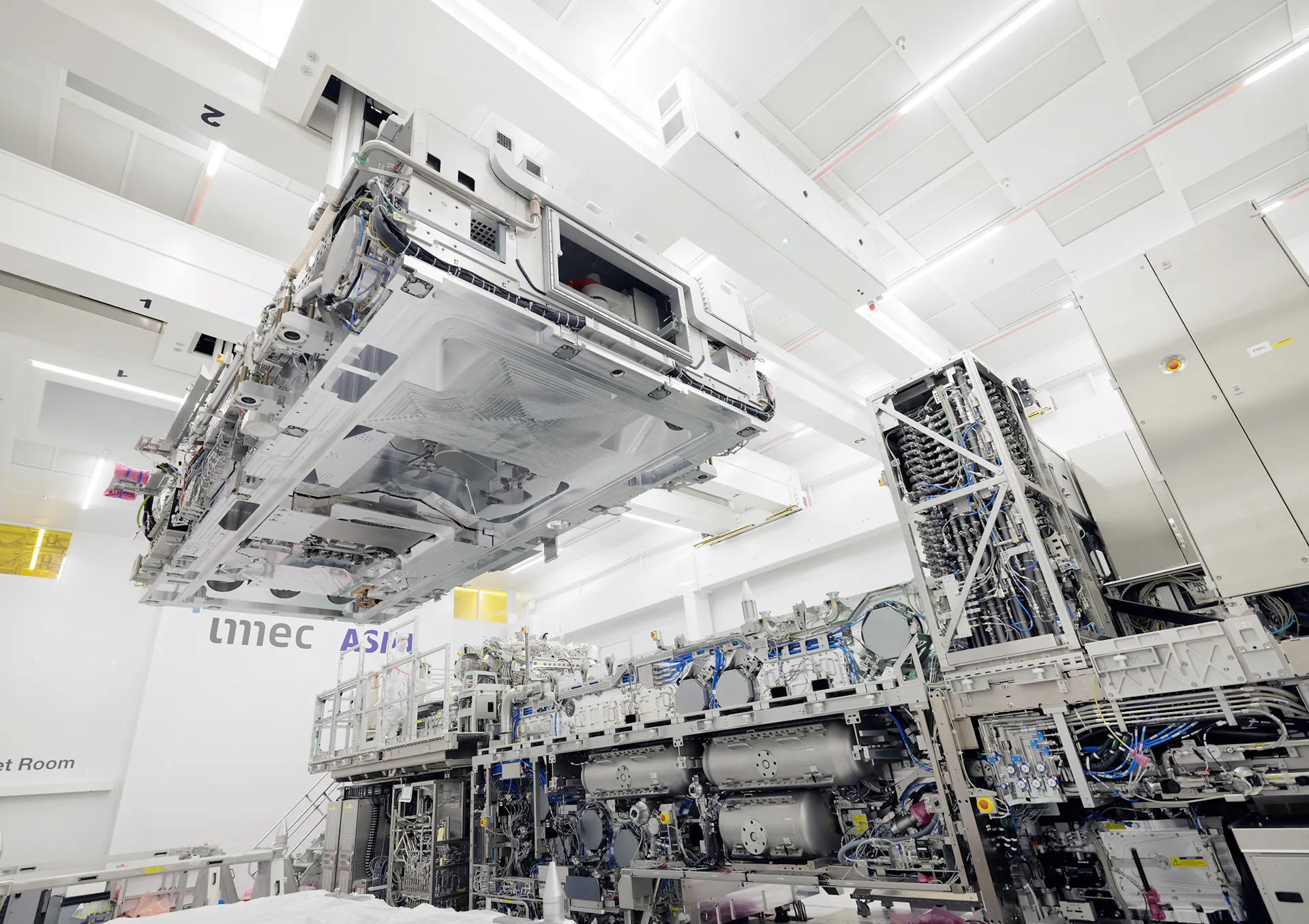
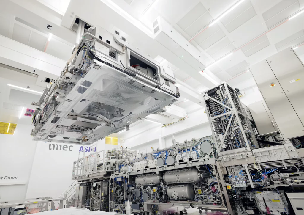
The ASML High NA Lab is a collaborative effort between ASML, a Dutch multinational corporation that develops and manufactures chip-making equipment, and imec, a world-leading research and development center for nanoelectronics and digital technologies. The lab is located in Veldhoven, Netherlands.
Follow us on LinkedIn for everything around Semiconductors & AI
The lab’s purpose is to accelerate the development and adoption of High NA EUV lithography. This is a next-generation technology that is expected to enable the production of even smaller and more powerful computer chips. EUV lithography (extreme ultraviolet lithography) is a type of photolithography that uses extreme ultraviolet light to create patterns on silicon wafers. High NA (high numerical aperture) refers to a property of lenses that determines how much light they can collect. In the context of EUV lithography, a higher NA lens can print smaller features on a chip.
The lab opened in June 2024 and is a $380 million investment. It provides leading-edge logic and memory chip makers, as well as advanced materials and equipment suppliers, access to the first prototype High NA EUV scanner (TWINSCAN EXE:5000). They also gain access to surrounding processing and metrology tools. This access allows them to experiment with the technology and develop new chipmaking techniques ahead of mass production.
Why does IMEC ASML Lab Matter:
Technological Advancement: The launch of the High NA EUV lab marks a significant milestone in semiconductor technology, with far-reaching implications for the industry. ASML’s new lab is poised to drive technological progress and innovation, ensuring a robust future for semiconductor manufacturing.
Competitive Edge: ASML’s collaboration with Imec and the development of the High NA EUV lithography tool reinforce its position as a leader in chip manufacturing. The enhanced capabilities of the tool will give chipmakers a competitive edge in producing cutting-edge semiconductor chips.
High NA EUV: Redefining Chip Manufacturing
High NA EUV lithography matters for a few key reasons: it allows for the creation of even smaller and more powerful computer chips.
Here’s a breakdown of its significance:
Smaller transistors, more powerful chips:
The core benefit of High NA EUV is its ability to print much finer features on a chip compared to previous generation EUV systems. This results in smaller transistors, which are the building blocks of a chip. Smaller transistors allow more to be packed onto a single chip, significantly increasing processing power and efficiency.
Pushing the limits of Moore’s Law:
Moore’s Law observes that the number of transistors on a microchip doubles roughly every two years. This principle is a cornerstone of the chip industry’s advancement. High NA EUV is critical for continuing this miniaturization trend. It allows chipmakers to stay on track with Moore’s Law for the foreseeable future.
Improved performance for various applications:
Smaller, more powerful chips benefit a wide range of applications. From faster smartphones and laptops to more powerful artificial intelligence and data centers, High NA EUV paves the way for significant advancements across various fields that rely on ever-increasing processing capabilities.
However, there are challenges:
High NA EUV technology is complex and expensive. Developing and implementing these systems requires significant investment and overcoming technical hurdles.
The High NA EUV lithography equipment is set to revolutionize chip manufacturing. It offers up to 60% better resolution compared to current EUV tools. This breakthrough will enable the creation of smaller, faster, and more efficient chips. It paves the way for advancements in various technology sectors.
ASML has reiterated its expectation that customers will begin commercial manufacturing with the High NA tool in 2025-2026. This timeline aligns with the company’s broader strategy to continue advancing its technology and maintaining its leadership position in the market.
Early Adoption and Orders
ASML has already shipped one test machine to Intel in the United States, with plans for incorporation into its 14A process by 2025. The strong interest in High NA tools is evident, with ASML receiving orders for more than a dozen units. While TSMC, ASML’s largest customer for EUV equipment, has indicated that it does not require High NA tools for its A16 chips, scheduled for production in 2025.