Introduction: Elevating Semiconductor Research and Development in Europe
In a remarkable endeavor that promises to reshape the landscape of semiconductor research and development in Europe, Applied Materials and the Fraunhofer Institute for Photonic Microsystems IPMS have announced a collaboration to create Europe’s largest technology hub for semiconductor metrology and process analysis.
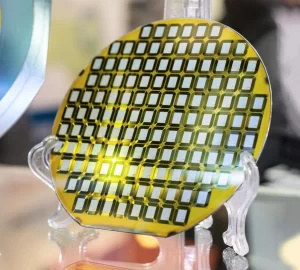
The hub will be located at the Center Nanoelectronic Technologies (CNT) of Fraunhofer IPMS in Dresden, Germany. It will be equipped with Applied Materials’ state-of-the-art eBeam metrology equipment, including its VeritySEM® CD-SEM (critical dimension scanning electron microscope) systems.
The hub will also be staffed by Applied engineers and R&D experts.
This groundbreaking collaboration aims to create what is projected to become Europe’s largest technology hub dedicated to semiconductor metrology and process analysis, with a specific emphasis on propelling research, innovation, and development within the ICAPS (Internet of Things, Communications, Automotive, Power, and Sensors) market segments.
Setting the Stage: The Strategic Location of the Technology Hub
The technology hub’s physical location at the Fraunhofer IPMS Center Nanoelectronic Technologies (CNT) is strategic on multiple fronts.
The CNT, known for providing applied research on 300mm wafers catering to microchip producers, suppliers, equipment manufacturers, and R&D partners, serves as the ideal host for this collaborative venture.
Moreover, the hub’s positioning within Silicon Saxony, Europe’s largest semiconductor cluster, adds another layer of significance, ensuring proximity to industry stakeholders and potential for cross-sector collaboration.
Empowering Innovation: Applied Materials’ Cutting-edge eBeam Metrology Equipment
At the heart of the collaborative effort lies the utilization of Applied Materials’ cutting-edge eBeam metrology equipment, including the VeritySEM CD-SEM (critical dimension scanning electron microscope) systems.
This sophisticated equipment is set to enable precise and comprehensive metrology processes, critical for ensuring the quality, efficiency, and functionality of semiconductor components.
Expertise at Work: The Role of Applied Engineers and R&D Specialists
The success of the technology hub heavily relies on the expertise and insights of the professionals involved. Applied Materials will deploy a team of skilled engineers and R&D specialists who will actively contribute to the operations and research conducted at the hub.
This fusion of technical excellence from both partners is expected to foster an environment of continuous learning, innovation, and collaborative problem-solving.
Read more: How IMEC made ASML the biggest company in Europe?
A Seamless Feedback Loop: Real-time Collaboration with Semiconductor Manufacturers
One of the standout features of the collaborative technology hub is Fraunhofer IPMS’s unique ability to directly collaborate with semiconductor manufacturers. This capability paves the way for real-time feedback loops, allowing for swift translation of research insights into practical industrial applications.
This seamless interaction between research and industry is poised to accelerate development cycles and enhance the efficiency of the innovation process.
The goal of the hub is to accelerate research and development in semiconductor metrology and process analysis.
It will also provide a platform for collaboration between chipmakers, equipment suppliers, and research institutes. The hub is expected to be operational in 2024.
Metrology is the science of measurement. In the semiconductor industry, metrology is used to measure the dimensions and properties of semiconductor materials and devices.
This information is essential for ensuring the quality and reliability of semiconductor products.
Process analysis is the study of the semiconductor manufacturing process. It is used to identify and understand the causes of defects and variations in semiconductor products.
Elevating Possibilities: A Glimpse into the Future
James Robson, Corporate Vice President for Applied Materials Europe, envisions the technology hub as a catalyst for accelerated learning cycles and the development of novel applications.
With the capability to test and qualify processes across diverse substrate materials and wafer thicknesses, the hub addresses the multifaceted needs of the European semiconductor landscape. This versatility is crucial as it allows for tailored solutions in various sectors such as IoT, communications, automotive, power, and sensors.
Here are some of the benefits of the new technology hub:
- It will accelerate research and development in semiconductor metrology and process analysis.
- It will provide a platform for collaboration between chipmakers, equipment suppliers, and research institutes.
- It will help to strengthen Europe’s position as a global leader in semiconductor manufacturing.
- It will create jobs and opportunities in the semiconductor industry.
Conclusion: Shaping the Future of European Semiconductor Innovation
The collaborative efforts between Applied Materials and the Fraunhofer Institute have laid the foundation for a groundbreaking technology hub that promises to reshape the semiconductor research and development landscape in Europe.
By merging cutting-edge equipment, technical expertise, and real-time collaboration with manufacturers, the hub is poised to fuel innovation, expedite development cycles, and foster invaluable partnerships.
As the technology hub takes shape, Europe’s position in the global semiconductor market is set to strengthen, ushering in a new era of advancements across industries and sectors.