Introduction
Taiwan Semiconductor Manufacturing Company (TSMC) is the world’s largest contract chipmaker and plays a critical role in the global semiconductor industry. However, TSMC has recognized the need to diversify its manufacturing footprint for several reasons both in Japan, USA and Germany.
In this blog post, we will explore the strategic move by TSMC to establish fabs in Japan and the United States, the challenges it faces, and the commitments it has made. Additionally, we’ll delve into the skilled labor shortage issues the company is confronting in both regions and the steps it’s taking to address them.
Follow us on Linkedin for everything around Semiconductors & AI
Diversifying Manufacturing Footprint
Reducing Reliance on Taiwan
TSMC currently houses all its manufacturing facilities in Taiwan, making it susceptible to political and economic risks in the region. To enhance its supply chain resilience, TSMC is seeking to reduce its reliance on Taiwan by building new fabs in other countries.
Meeting Growing Demand
The global demand for semiconductors has been skyrocketing, and TSMC is struggling to keep up with the surge. By establishing new fabs in Japan and the US, the company aims to increase its production capacity and cater to the rapidly growing demand.
Responding to Government Pressure
Both the US and Japanese governments have been urging TSMC to invest in their countries. The US is concerned about its dependency on foreign chipmakers and wants to strengthen its semiconductor industry. Similarly, Japan seeks to secure a stable supply of semiconductors and reduce reliance on foreign manufacturers.
Also Read: China orders $5B of Nvidia’s processors amid fear of US ban
TSMC Japan and US Fabs: Notable Differences
The two fabs exhibit some notable differences in terms of partnerships, process technology, capacity, and locations.
TSMC Japan:
- The Japan project is a joint venture between TSMC and Sony. The plant will be used to produce chips for both companies.
- Use of older process technology (12nm, 16nm, and 22nm).
- The Japanese government has offered TSMC a large subsidy for the fab, which could make it difficult for other chipmakers to compete.
- Remote location, which could affect workforce recruitment.
TSMC Arizona:
- The Arizona project is being built by TSMC alone. The plant will be used to produce chips for a variety of customers, including Apple, Qualcomm, and Nvidia.
- Advanced process technology (4nm and 3nm).
- Located in a desert area, potentially posing water supply challenges.
How 2 projects differ
TSMC Japan
- Sony’s involvement will give TSMC access to Sony’s expertise in the semiconductor industry. Sony is a major player in the semiconductor industry, and it has a strong track record of innovation. TSMC’s partnership with Sony will give TSMC access to Sony’s expertise in areas such as design, manufacturing, and marketing.
- The partnership will also give TSMC a foothold in the Japanese market. Japan is a major market for semiconductors, and it is home to a number of major semiconductor companies. TSMC’s partnership with Sony will give TSMC a stronger presence in the Japanese market.
TSMC Arizona
- Building the Arizona fab alone will give TSMC more control over the project. TSMC will be able to make all of the decisions about the design, construction, and operation of the fab. This will give TSMC more flexibility and control over the project.
- Building the fab alone will also allow TSMC to save money. TSMC will not have to share the costs of the project with a partner. This will allow TSMC to invest more money in the fab and to keep the costs down.
Read more: TSMC and Arizona Take Action to Protect Workers in Semiconductor Manufacturing
Commitments Made by TSMC
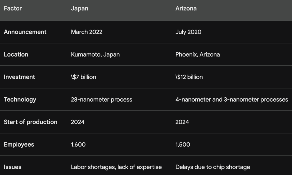
TSMC Japan:
- Investment of $7 billion.
- Fab capacity of 50,000 wafers per month.
- Utilization of 12nm, 16nm, and 22nm processes.
TSMC Arizona:
- Investment of $12 billion.
- Fab capacity of 20,000 wafers per month.
- Utilization of 4nm and 3nm processes.
Challenges Faced by TSMC
Labor Shortages
One of the primary challenges both projects face is labor shortages. In both Japan and Arizona, there is a limited pool of semiconductor expertise, which poses difficulties in recruiting skilled workers for the fabs.
Lack of Expertise in Japan
The Japan project faces an additional hurdle due to a lack of expertise in the 28-nanometer process, which is no longer widely used. This poses challenges in finding experienced personnel and could potentially impact project timelines.
Delays Due to Chip Shortage
The Japan project has faced delays due to the ongoing global chip shortage, affecting the procurement of essential components and slowing down the progress of the fab construction.
Skilled Labor Shortage Issues
Global Shortage of Skilled Workers
The semiconductor industry worldwide is grappling with a scarcity of skilled workers due to the highly technical nature of the field and the cyclical nature of the industry.
Japan:
- Acute skilled labor shortage due to an aging and shrinking population.
- Attracting and retaining skilled workers in the remote Kumamoto area is challenging, despite the subsidy offered by the Japanese government.
Arizona:
- A lesser but still significant skilled labor shortage in the Phoenix area.
- TSMC is building a training center at the fab to equip workers with the necessary semiconductor manufacturing skills.
TSMC’s Steps to Address Skilled Labor Shortage
- Collaborating with universities to train students in semiconductor manufacturing.
- Offering competitive salaries and benefits to attract and retain skilled workers.
- Building a training center at the Arizona fab to upskill the local workforce.
Conclusion
TSMC’s move to expand its manufacturing footprint to Japan and the US is a strategic response to diversify its operations, meet growing semiconductor demand, and respond to government pressures.
The Japanese fab will help to ensure that Japan has a secure supply of semiconductors, while the Arizona fab will help to boost the U.S. semiconductor industry. However, both fabs face challenges, and it remains to be seen how successful they will be.
However, the challenges of skilled labor shortages and other regional-specific issues pose hurdles that the company must overcome to ensure the success of these crucial projects. TSMC’s efforts to address these challenges will play a crucial role in shaping the future of the global semiconductor industry.