Introduction
In 1984, a year that witnessed the groundbreaking emergence of personal computing with IBM’s PC and Apple’s inaugural Macintosh release, a different kind of revolution was unfolding in Leuven, Belgium.At the same time these iconic tech moments occurred, IMEC was born, driven by a group of forward-thinking young researchers.
Some of these visionaries had experienced the transformative wave of innovation in Silicon Valley, which ignited their aspirations for a similar revolution on their home turf.
Empowered by generous funding from the regional Flemish government, they embarked on a mission to establish an electronics superlab that would catalyze an industrial renaissance in Flanders.
The founders of imec harbored an ambitious vision: to continually shrink, enhance the power of, and improve the energy efficiency of CMOS computer chips.
Their aim was to solidify Gordon Moore’s prophetic observation into an undeniable law—an evolution that would see the capabilities of integrated circuits double every 24 months.
imec has consistently demonstrated growth, a testament to the efficacy of its partnership-driven model in bestowing stability upon an inherently cyclic semiconductor landscape.
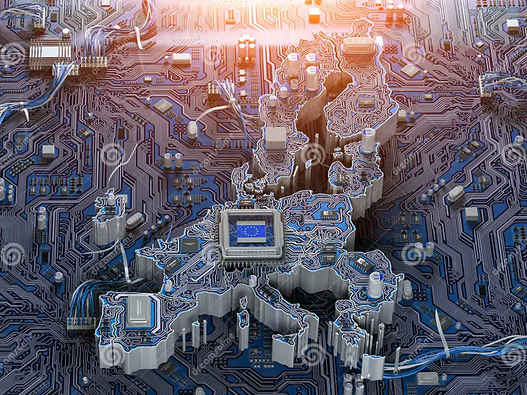
IMEC stands as a reliable collaborator for enterprises, startups, and educational institutions, uniting more than 4,000 exceptional individuals. This diverse community represents nearly 100 nationalities, both on-site and through distributed research and development units spanning Flemish and Dutch universities, as well as locations in Taiwan, the USA, China, India, and Japan. As of 2018, IMEC achieved a revenue of 583 million euros.
Founding and Vision
The roots of imec trace back to a time when the Flemish government recognized the potential of microelectronics to drive economic growth. With the aim of bolstering the semiconductor industry within the relatively small Flanders district, a comprehensive program was devised.
This program consisted of three integral components: an advanced research laboratory, a semiconductor foundry, and a training program for Very Large Scale Integration (VLSI) design.
In 1984, the advanced research laboratory was formalized as imec, a nonprofit organization headquartered in Leuven, Belgium.
Imec’s core mission was to engage in forward-looking research and development that anticipated industrial needs by 3-10 years.
This bold approach positioned imec at the forefront of technological innovation, focusing initially on microelectronics and design, and later expanding into diverse fields such as energy.
Read More:Follow us on Linkedin for everything around Semiconductors & AI
Then & Now
Back in 1984, imec started as a small lab with a bit of money and a big dream. They invested a lot in having the right tools and facilities, like special rooms to make electronics.
Companies quickly saw the potential in imec and wanted to work with them. One reason was that imec had friends in the tool-making business, which meant they could use the latest and greatest tools for their work.
Imec wanted to help companies that make computer chips and tools to be the best in the race to make better chips on bigger wafers.
They didn’t just do their own thing; they worked with lots of other companies to solve problems together before they even became problems.
When they started, there were about 70 people working at imec. Now, they’ve grown to have around 5,000 people.
The money they make has also grown a lot – from a little bit to more than 700 million euros.
Most of this money comes from working closely with companies, which is much more than the help they get from the Flemish government. This help is really important because it lets imec do deeper research and create ideas that others haven’t thought of.
Today, making computer chips that work really well is a big challenge. It’s even harder because of things like big data, AI, and the Internet of Things.
But imec has changed from just helping companies to a super important place where people from all around the world meet up to make technology better for everyone.
Read More:Explained: What is CMOS Technology? – techovedas
Leadership and Expertise
At its inception, imec was led by Professor Roger Van Overstraeten, a distinguished Stanford Ph.D. graduate from the Catholic University of Leuven. Under his guidance, imec swiftly assembled a team of researchers, engineers, and innovators who shared an unwavering commitment to advancing the boundaries of microelectronics technology.
Here are the top 5 big achievements of Imec
- The development of extreme ultraviolet (EUV) lithography.
- The development of new materials for electronics, such as graphene, silicon carbide, and III-V semiconductors.
- The development of new imaging technologies, such as near-field scanning optical microscopy (NSOM), atomic force microscopy (AFM), and electron microscopy.
- The development of new energy technologies, such as solar cells, batteries, and fuel cells.
- The development of new healthcare technologies, such as medical imaging, diagnostics, and drug delivery.
Industry affiliate programme
The Industrial Affiliation Program operates as a collaborative business model that facilitates the shared funding of development efforts among multiple partners.
This framework brings together researchers from both industries and imec to concentrate on advancing specific technologies.
imec provides a neutral environment where these parties can work collaboratively within well-defined project scopes and established rules concerning ownership of intellectual property (IP).
Various stakeholders across the value chain, including foundries, fabless designers, tool manufacturers, and EDA providers, collaborate to construct a unified platform. The expenses related to developing this technology, which can be substantial, are collectively distributed. Meanwhile, the rights to valuable IPs are divided either through shared arrangements or exclusive ownership, depending on the method of discovery.
This dynamic resembles the concept of producing a Hollywood film. Different experts like directors, actors, set designers, and costume designers come together with a substantial budget to closely collaborate on a singular project.
The value generated by these intellectual properties is shared among the participants, following predetermined rules. At the conclusion of the project, each entity goes their separate ways.
imec generates revenue through these partnerships, both for participating in the collaborations and for the original IPs it contributes to the endeavor. The IPs imec identifies and possesses through these partnerships are subsequently utilized to initiate new cooperative ventures.
imec’s Pivotal Role in ASML’s EUV Lithography Success
imec played a significant role in facilitating ASML’s journey towards commercializing Extreme Ultraviolet (EUV) lithography. Long before any EUV prototype was even developed, imec collaborated extensively with the six major photoresist manufacturers in the industry to discover an appropriate EUV photoresist.
Since a suitable tool wasn’t available yet, imec conducted its tests using EUV radiation generated by a synchrotron at the Paul Scherrer Institute in Switzerland.
In August 2006, ASML achieved a breakthrough by creating the first comprehensive, full-field EUV lithography machine known as the Alpha Demo Tool.
Among the first two recipients of this tool from ASML were imec and the College of Nanoscale Science and Engineering of the State University of New York at Albany. The latter institution’s name is quite a mouthful.
imec’s objective with this demonstration tool was twofold: to assess its commercial viability by utilizing progressively more advanced process nodes and concurrently identify crucial challenges in the tool, photoresist, and photomask.
In 2011, imec received the NXE:3100 from ASML, and they collaborated closely with laser supplier Ushio to enhance the tool’s wafer throughput and minimize defects.
Integrated tool
As EUV technology moved closer to practical implementation, imec utilized its accumulated knowledge to aid chipmakers in seamlessly integrating the tool into their processes.
- IMEC developed the first EUV light source, which is a critical component of the machine.
- IMEC developed the first EUV optics, which are used to focus the light onto the semiconductor wafer.
- IMEC worked with ASML to develop the software that controls the EUV machine.
- IMEC continues to collaborate with ASML on the development of new EUV lithography technologies.
As a result of IMEC’s contributions, ASML is now the only company in the world that manufactures EUV lithography machines. They have a monopoly on this technology, and they are the only company that can supply the semiconductor industry with the machines they need to make the most advanced chips.
This gives ASML a lot of power in the semiconductor industry, and it makes them a very important player.
Presently, with EUV technology integrated into foundries, imec researchers are engrossed in projecting future process nodes and addressing intricate concerns such as stochastic printing failures in EUV.
Read more: How ASML’s EUV Lithography Technology Made It Europe’s Most Valuable Company
Conclusion
Imec’s journey from a government-initiated program to a global powerhouse of microelectronics research exemplifies the potential of strategic vision and proactive investment in technological innovation.
Its partnership with ASML stands as a model for how collaboration between research institutions and industry giants can result in mutual success and drive the advancement of entire industries.
The tale of imec is an inspiring narrative that underscores the importance of research, foresight, and determination in shaping the future of technology.