Introduction
The semiconductor industry is witnessing a fierce battle for supremacy in the Angstrom Arena as major players like TSMC, Intel, and Samsung unveil their next-generation processes to redefine the boundaries of performance, efficiency, and innovation.
In this high-stakes competition, each company aims to outshine its rivals with cutting-edge technology and strategic advancements.
A16, 14A, and SF 1.4 all refer to chip manufacturing processes, specifically the size at which transistors are built on the chip.
What are TSMC A16, Intel 14A and Samsung SF1.4
A16 (TSMC): This is an upcoming process from TSMC (Taiwan Semiconductor Manufacturing Company), a leading chip manufacturer. The “A16” signifies it uses an angstrom-class measurement, which is smaller than the nanometer (nm) scale used traditionally. This allows for transistors to be packed much tighter, potentially leading to significant performance and efficiency improvements.
14A (Intel): This is Intel’s upcoming process. The “14” refers to 14 nanometers, the size of the transistors. The “A” likely indicates advancements over previous 14nm processes Intel offered, but specifics are unclear.
SF 1.4 (Samsung): Similar to Intel’s 14A, Samsung’s SF 1.4 is also a 14nm process. The “SF” might stand for “Second Foundry” or a specific internal code, and “1.4” likely signifies an improvement over previous 14nm processes from Samsung.
Difference:
Manufacturing lead: TSMC’s A16 process, an angstrom-class technology, represents a significant leap forward compared to Intel’s 14A and Samsung’s SF1.4, which both remain in the 14nm range. This advancement allows TSMC to pack transistors much tighter, potentially leading to better performance and efficiency.
Production timeline: TSMC is aiming for mass production of the A16 in 2026, ahead of both Intel’s 14A and Samsung’s SF1.4 which are slated for 2027.
Cost advantage: A major advantage of the A16 process is that it doesn’t require High-NA EUV lithography, which is an expensive technology. This could make TSMC’s chips more cost-competitive.
Follow us on Linkedin for everything around Semiconductors & AI
TSMC’s A16: Leading the Charge
TSMC’s A16 advanced process steals the spotlight with its early mass production schedule set for 2026, trumping competitors Intel and Samsung, whose offerings are slated for 2027.
What sets the A16 apart is its ingenious combination of Super PowerRail and nanosheet transistors, promising unparalleled performance and cost-effectiveness.
The incorporation of Super PowerRail technology, which relocates power networks to the backside of wafers, allows for enhanced logic density and performance, particularly beneficial for high-demand applications like High-Performance Computing (HPC) products.
Moreover, TSMC’s decision to forgo the use of High-NA EUV underscores its commitment to cost competitiveness without compromising on performance, positioning the A16 as an attractive option for clients seeking optimal value.
Performance and Efficiency: TSMC claims the A16 offers an 8% to 10% speed increase and a 15% to 20% reduction in power consumption compared to their previous N2P process.
Applications: The A16 is particularly suited for High-Performance Computing (HPC) due to its focus on dense logic integration and power delivery.
Read More:AI GPU Market 2024: NVIDIA dominates with $40B, AMD rises to $3.5B, Intel lags at $500M – techovedas
Intel’s 14A: Driving Innovation Forward
Intel enters the fray with its 14A process, marking a significant milestone in its “5 Nodes in 4 Years” strategy.
By integrating High-NA EUV production, Intel aims to achieve remarkable improvements in energy efficiency and transistor density compared to its predecessors.
Additionally,the introduction of Intel 14A-E further amplifies the company’s commitment to innovation, promising a 5% increase in energy efficiency over the base 14A process.
Intel’s emphasis on the integration of High-NA EUV lithography tools underscores its dedication to pushing the boundaries of technology, ultimately enhancing its process roadmap and solidifying its position as a key player in the semiconductor arena.
Read More: 8 Companies Poised to Benefit Significantly from the AI Boom – techovedas
Samsung’s SF1.4: Embracing Nanosheet Technology
Samsung joins the competition with its SF1.4 process, leveraging nanosheet technology to enhance performance and power efficiency. Although lagging slightly behind TSMC and Intel in the timeline, Samsung’s strategic advancements in nanosheet technology position SF1.4 as a contender in the race for semiconductor supremacy.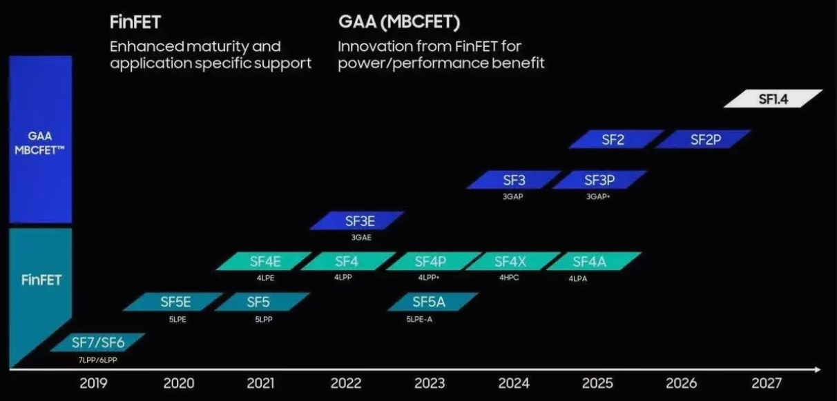
By increasing the number of nanosheets per transistor, such as Samsung aims to optimize drive current, improve performance, and reduce power consumption.
Moreover, this innovative approach reflects Samsung’s commitment to driving technological progress and remaining competitive in the dynamic semiconductor landscape.
Read More: Level Up Your Electronics: 7 Types of Arduino Boards to Make Your Own Gadget – techovedas
Comparison of TSMC A16 with Intel 14A and Samsung SF1.4
Comparison of TSMC’s A16, Intel’s 14A, and Samsung’s SF1.4 in the Angstrom Era
In the fast-paced world of semiconductor manufacturing, TSMC’s A16, Intel’s 14A, and Samsung’s SF1.4 stand as titans, each vying for dominance in the Angstrom Arena
This comparison table provides a comprehensive overview of their key features and specifications, offering insights into their respective strengths and advantages.
| Feature | TSMC A16 | Intel 14A | Samsung SF1.4 |
|---|---|---|---|
| Mass Production Date | 2026 | 2026 (14A) / 2027 (14A-E) | 2027 |
| Key Technology | Super PowerRail, Nanosheets | High-NA EUV | Nanosheet |
| Power Efficiency | 15-20% reduction in power consumption | 15% improvement (14A) / 5% improvement (14A-E) | Not specified |
| Transistor Density | Up to 1.1 times increase | 20% increase | Not specified |
| Compatibility | Ideal for HPC products | Wide range of applications | Performance and power efficiency focus |
| High-NA EUV Required | Not required | Yes | Not specified |
Deep Dive: TSMC A16 vs Intel 14A vs Samsung SF 1.4
While all three are upcoming chip manufacturing processes, here’s a detailed comparison based on the information available:
Process Node:
- TSMC A16: Angstrom-class (specific number not publicly disclosed)
- Intel 14A: 14nm (though the “A” likely signifies advancements over previous 14nm nodes)
- Samsung SF1.4: 14nm (similar to Intel, details on improvements over prior 14nm processes are scarce)
Transistor Density:
- TSMC A16: Expected to be significantly higher due to the angstrom-class design, allowing for more transistors packed into a smaller area. This translates to potentially better performance.
- Intel 14A & Samsung SF1.4: Lower transistor density compared to A16 due to the 14nm node.
Manufacturing Timeline:
- TSMC A16: Mass production targeted for 2026.
- Intel 14A & Samsung SF1.4: Production expected in 2027.
Cost:
- TSMC A16: Potentially more cost-competitive because it doesn’t require High-NA EUV lithography, an expensive technology.
- Intel 14A & Samsung SF1.4: Cost details unclear, but EUV usage might make them pricier.
Performance & Efficiency:
- TSMC A16: TSMC claims 8-10% speed increase and 15-20% power reduction compared to their N2P process.
- Intel 14A & Samsung SF1.4: Specific performance and efficiency gains haven’t been disclosed by either company. However, due to the larger node size, they might not match A16’s potential.
Applications:
- TSMC A16: Focuses on dense logic integration and power delivery, making it ideal for High-Performance Computing (HPC).
- Intel 14A & Samsung SF1.4: Applications unclear without more details from the companies. They might target a broader range including CPUs, GPUs, and mobile processors depending on their specific optimizations.
Unknowns:
- Specific details about transistor types and architectural improvements for each process are not yet public.
- Real-world performance and efficiency comparisons will need to wait for benchmark testing after these chips are manufactured.
Overall:
TSMC’s A16 appears to be a significant leap forward with its angstrom-class design and potential performance/efficiency gains. The earlier production timeline and potentially lower cost due to not requiring High-NA EUV are further advantages. However, Intel and Samsung might have their own optimizations planned for their 14A processes, so the final picture won’t be clear until all chips hit the market.
Read More: Breakthrough! NVIDIA Optimizes All Platforms for Blazing-Fast Meta Llama 3 – techovedas
Conclusion:
As TSMC A16, Intel 14A, and Samsung SF1.4 vie for dominance in the Angstrom Arena, the semiconductor industry stands at a pivotal juncture in its evolution.
Additionally, these advancements not only herald a new era of computing but also underscore the collaborative spirit driving progress in semiconductor technology.
Moreover, as the battle of the titans unfolds, one thing remains certain: the Angstrom Era heralds a new dawn of possibility, where innovation knows no bounds.
Whether it’s pioneering new manufacturing processes, optimizing performance and efficiency, or embracing emerging technologies, each player contributes to a collective vision of a future where computing transforms lives and shapes the world.