Introduction
The realm of chip design is on the brink of a revolution with the advent of CMOS 2.0. Moreover, this groundbreaking approach promises to redefine the boundaries of semiconductor technology, offering a glimpse into a future where computing power knows no bounds.
This blog post delves into the core principles of CMOS 2.0, explores its potential functions and future applications, and sheds light on its significance for the technological landscape.
Follow us on Linkedin for everything around Semiconductors & AI
Understanding the Need for Change: The Evolution of CMOS Technology
For decades, CMOS technology has served as the bedrock of semiconductor design, fueling the exponential growth of computing capabilities. However, the relentless pursuit of miniaturization has brought forth a host of challenges, including escalating power consumption, diminishing performance gains, and soaring fabrication costs. Moreover, as the traditional CMOS approaches the limits of scalability, the need for a paradigm shift becomes increasingly apparent.
Read More: Explained: What is CMOS Technology? – techovedas
What is CMOS 2.0?
CMOS (Complementary Metal-Oxide-Semiconductor) has been the cornerstone of chip design for decades. However, as we approach the limits of miniaturization and face challenges like power dissipation and performance bottlenecks, the need for innovation has become more pressing than ever. This is where CMOS 2.0 steps in.
Core Functions of CMOS 2.0:
While the specific details of various CMOS 2.0 implementations are still under development, some of the key functionalities envisioned include:
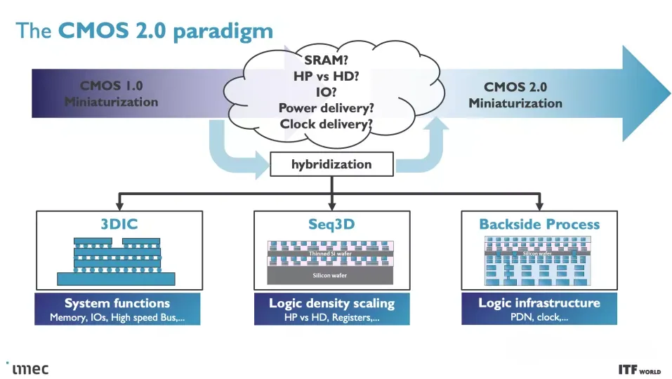
- Heterogeneous Integration: This involves combining different materials and device types on a single chip, enabling the integration of logic, memory, and other functionalities on a single die. Moreover,this can lead to significant performance improvements and miniaturization.
- Three-Dimensional (3D) Stacking: This technology allows for stacking multiple layers of transistors vertically, providing more real estate for complex circuits without increasing the physical footprint of the chip. Moreover,this can lead to denser chips with enhanced functionality.
- Advanced Materials: Incorporating new materials like gallium nitride (GaN) and wide-bandgap semiconductors can offer superior properties like higher efficiency and improved performance compared to traditional silicon.
- Neuromorphic Computing: This involves designing chips that mimic the structure and function of the human brain, enabling more efficient processing of complex data patterns and potentially revolutionizing fields like artificial intelligence.
Read More: What are the challenges faced by Modern CMOS scaling? – techovedas
The Future of CMOS 2.0:
The potential applications of CMOS 2.0 are vast and encompass various industries:
- Artificial Intelligence (AI): Neuromorphic chips can significantly accelerate AI development, enabling faster training of complex algorithms and paving the way for more advanced AI applications.
- Internet of Things (IoT): The miniaturization and power efficiency benefits of it can empower the development of smaller, more energy-efficient IoT devices, fostering the growth of the interconnected world.
- High-Performance Computing (HPC): Advanced chip architectures enabled by it can unlock new levels of computing power, facilitating complex scientific simulations and data analysis.
- Consumer Electronics: The potential for denser, more efficient chips can lead to sleeker, more powerful smartphones, laptops, and other consumer devices.
The Importance of CMOS 2.0:
The CMOS 2.0 revolution holds immense significance for the future of technology:
- Addressing Scalability Challenges: As traditional CMOS approaches its physical limitations, CMOS 2.0 offers a pathway to overcome these hurdles and continue the miniaturization and performance scaling of chips.
- Enhancing Efficiency: New materials and device structures can lead to significant improvements in power efficiency, moreover a crucial factor in the development of sustainable and eco-friendly technologies.
- Driving Innovation: The possibilities unlocked by CMOS 2.0 can pave the way for entirely new chip architectures and functionalities, fostering innovation across various scientific and technological disciplines.
Read More: CMOS: From Overlooked Innovation to Semiconductor Dominance – techovedas
Conclusion:
The CMOS 2.0 revolution presents a transformative chapter in the history of chip design.However, By embracing new materials, device structures, and design paradigms, it has the potential to address current limitations, unlock new functionalities, and propel the technological landscape towards a brighter future. As research and development in this domain continue to evolve, the true impact of CMOS 2.0 is yet to be fully realized, but its potential to shape the future of technology is undeniable.