Introduction
The semiconductor industry is at the heart of modern technology, driving innovation and enabling the creation of smaller, faster, and more powerful devices. One of the key processes in semiconductor manufacturing is lithography, which involves the precise patterning of silicon wafers to create intricate integrated circuits.
Over the years, several groundbreaking patents have revolutionized lithography, pushing the boundaries of what is possible and enabling the continued miniaturization of transistors.
Here, we explore five pivotal lithography-related patents that have significantly impacted the semiconductor industry.
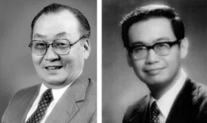
1. Phase-Shifting Masks (US Patent 4,493,601) – 1984, by David Markle
In the early stages of lithography, as semiconductor technology advanced, there was a constant push to create smaller and more densely packed transistors.
Moore’s Law, a commonly cited trend, predicts that the number of transistors on a chip will double approximately every two years.
Achieving this miniaturization required increasingly precise patterning techniques.
In optical lithography, the diffraction limit poses a significant challenge, determined by the wavelength of the light used and the numerical aperture (NA) of the imaging system.
As the feature sizes on semiconductor wafers approached the wavelength of the light used for exposure, diffraction effects became more pronounced.
These effects caused the printed patterns to blur and lose resolution, making it difficult to create small, distinct features accurately.
The Solution: Phase-Shifting Masks (PSMs)
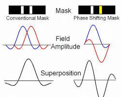
David Markle’s introduction of phase-shifting masks (PSMs) in 1984 provided a groundbreaking solution to this problem.
The core idea behind PSMs is to manipulate the phase of the light passing through the mask to enhance the resolution of the printed features. Here’s a detailed explanation of how phase shifters addressed the issue:
Diffraction and Interference:
- Diffraction: When light passes through an opening (such as the features on a mask), it bends and spreads out. This spreading causes adjacent features to blur together, especially when the feature sizes are close to the wavelength of the light.
- Interference: Light waves can interfere with each other constructively (amplifying the light) or destructively (canceling the light) based on their phase relationships.
Phase Manipulation:
- Traditional masks allow light to pass through transparent areas and block it in opaque areas. This approach relies solely on the intensity of the light to define features.
- Phase-shifting masks introduce a phase shift in the light passing through different parts of the mask. By shifting the phase of the light by 180 degrees (half a wavelength), researchers can induce light waves to interfere destructively at the edges of features, thereby creating sharper transitions and higher contrast.
Enhanced Resolution:
- In a PSM, specific areas of the mask are designed to introduce this phase shift. When light passes through these areas, it undergoes constructive or destructive interference with light from adjacent areas.
- Destructive interference at the edges of features sharpens the image, reducing the effects of diffraction and effectively enhancing the resolution of the printed pattern.
Implementation of PSMs:
- Alternating PSMs: This technique uses two different phase levels, typically 0 degrees and 180 degrees. These masks create alternating transparent regions that yield high-contrast images because of the destructive interference at their boundaries.
- Attenuated PSMs: These masks partially transmit light and also shift its phase, providing a combination of phase shifting and attenuation to achieve improved imaging.
2. Immersion Lithography (US Patent 5,043,282) – 1991, by Canon

In 1991, Canon introduced a revolutionary approach with its patent on immersion lithography. This technique involved placing a liquid immersion medium between the lens and the wafer during the lithography process. The immersion medium increased the numerical aperture (NA) of the lens system, leading to higher resolution. Immersion lithography significantly extended optical lithography capabilities. It enabled further miniaturization of transistors. This advancement boosted the overall performance of integrated circuits.
Canon’s 1991 patent on immersion lithography introduced an innovative solution to overcome the resolution limitations of traditional optical lithography. Here’s a detailed explanation of how immersion lithography addressed these issues:
Read More:IBM and Pasqal Forge Open-Source Path to Build Practical Quantum Supercomputers. – techovedas
Numerical Aperture and Refractive Index:
- The numerical aperture (NA)(NA)(NA) is directly proportional to the refractive index (n)(n)(n) of the medium between the lens and the wafer.
- In traditional optical lithography, air (with a refractive index of approximately 1) serves as the medium.This limits the maximum NANANA to values less than 1.
Introducing a Liquid Immersion Medium:
- Immersion lithography replaces the air gap between the lens and the wafer with a liquid immersion medium, typically water, which has a higher refractive index (around 1.44 for water).
- Using a liquid medium significantly increases the effective NANANA, enabling greater resolution.
Enhanced Resolution:
- This emphasizes the direct relationship between increasing NANANA and the reduction in minimum feature size. A higher NANANA effectively lowers the diffraction limit, enabling the patterning of smaller features.
- This improvement is crucial for producing advanced semiconductor devices with smaller transistors and higher circuit densities.
Read More: Upto 22% : Top 5 Semiconductor Equipment Makers Sales Surge in Q1 2024 – techovedas
3. EUV Lithography (US Patent 5,753,491) – 1998, by ASML
As semiconductor technology progressed, the drive to create smaller and more densely packed transistors intensified. The resolution limit imposed by the wavelength of light used in the lithography process posed a key challenge. While advancements like 193nm immersion lithography have pushed boundaries, creating smaller chip features is hitting a physical barrier. To continue miniaturization and meet Moore’s Law demands, moving to even shorter wavelengths of light became necessary.

The shorter the wavelength, the finer the details that can be resolved. However, moving to extreme ultraviolet (EUV) wavelengths, specifically 13.5nm, introduced significant technical challenges:
- Light Source: Generating stable, powerful EUV light sources.
- Optics: Designing reflective optics and masks that could handle EUV without absorbing the light, as most materials absorb EUV wavelengths.
- Contamination: Managing contamination, as EUV systems are extremely sensitive to particles and other contaminants.
Read More: Rapidus and IBM Collaborate for Chiplet Packaging for 2nm Process Node – techovedas
The Solution: Phase-Shifting Techniques in EUV Lithography
While the use of phase shifters in EUV lithography is less straightforward than in traditional optical lithography, phase-shifting techniques still play a crucial role in enhancing resolution and image contrast. Here’s how phase-shifting principles are applied to address the issues in EUV lithography:
Mask Design:
- Phase Shifting Masks (PSMs): Even in the context of EUV, masks can be designed to incorporate phase-shifting elements. These masks manipulate the phase of the reflected EUV light to enhance image contrast and resolution.
- Absorber Patterns:Absorber patterns in EUV masks are engineered to modify the phase of the EUV light upon reflection, similar to how conventional PSMs function with transmitted light. Engineers fine-tune these patterns to generate constructive and destructive interference, thereby enhancing the sharpness of the features.
Read More: Expedera Opens Sixth Global R&D Center in Hyderabad, India: Implications – techovedas
Reflective Optics:
- Unlike traditional optical lithography, which uses lenses, EUV lithography relies on reflective optics due to the high absorption of EUV wavelengths by most materials. These mirrors must be coated with multilayer materials (such as molybdenum/silicon) to reflect EUV light efficiently.
- Phase-shifting techniques can also be applied in the design of these multilayer mirrors to control the phase of the reflected light and enhance the overall resolution of the system.
Image Contrast and Resolution:
- The application of phase-shifting principles in EUV lithography helps to manage the phase of light waves, ensuring that the interference patterns produce higher contrast and better-defined features on the wafer.
- Achieving the high resolution required for advanced semiconductor devices is critical, especially considering features much smaller than what can be achieved with 193nm lithography.
Follow us on Twitter: https://x.com/TechoVedas
Conclusion
The evolution of lithography technology has been instrumental in the advancement of the semiconductor industry. From phase-shifting masks to EUV lithography, each innovation has pushed the limits of what is possible, enabling the creation of smaller, faster, and more powerful integrated circuits. These five patents represent significant milestones in lithography, driving the progress of modern electronics and shaping the future of technology. As the industry continues to evolve, we can expect further breakthroughs in lithography to continue revolutionizing the world of semiconductors.