Introduction
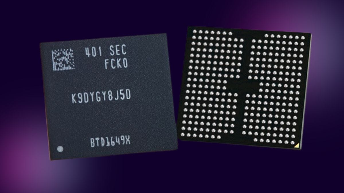
Samsung Electronics, a pioneer in advanced memory technology, has officially announced the commencement of mass production for its groundbreaking one-terabit (Tb) triple-level cell (TLC) 9th-generation vertical NAND (V-NAND).
This milestone solidifies Samsung’s position as the global leader in the NAND flash market and heralds a new era of innovation in storage solutions.
SungHoi Hur, Head of Flash Product & Technology at Samsung Electronics, expressed excitement about the industry’s first 9th-gen V-NAND, highlighting its potential to propel future applications forward. He emphasized Samsung’s commitment to pushing the boundaries in cell architecture and operational schemes to meet the evolving needs of NAND flash solutions, particularly in anticipation of the demands of the AI generation.
Industry-leading: Samsung claims this is the first and most advanced V-NAND memory available.
Higher capacity: The new design offers a 1 terabit (Tb) capacity, which is a significant improvement over previous generations.
Faster data transfer: Samsung says the new V-NAND can achieve data transfer rates as high as 3.2 GT/s.
Lower power consumption: The design is 10% more energy efficient than the previous generation.
Applications: This new V-NAND is expected to be used in high-performance solid state drives (SSDs).pen_spark
Follow us on Linkedin for everything around Semiconductors & AI
Background:
The timeline of the human species pales in comparison to just 14 seconds when mapped onto the expansive history of the universe. With over 170 billion known galaxies continuously expanding, it’s evident that neither the Sun nor Earth holds a central position in universal development. Similarly, semiconductor technology reflects this grand scale.
Using an electron microscope, one can peer into a miniature universe encapsulated within a semiconductor chip smaller than a fingernail. Despite its diminutive size, a chip merely 1mm thick contains millions of meticulously engineered spaces to store vast amounts of data.
Traditionally, NAND flash memory solutions employed a two-dimensional (2D) architecture, stacking chips on flat surfaces. However, this approach severely limited data storage capacity.
Addressing this constraint required significant research, leading to Samsung’s breakthrough invention of V-NAND (vertical memory) flash memory. This technology stacks cell layers vertically, connected via perforations in 3D space. Samsung emerged as the pioneer in designing and marketing such a memory solution.
The introduction of 3D V-NAND revolutionized memory semiconductors, moving away from the flat 2D structures dominant in electronic storage for decades. This transition is akin to people shifting from single- or two-story residences to high-rise apartments for the first time.
Samsung’s Semiconductor Solution Victory: V-NAND
Since its groundbreaking debut, the V-NAND solution, featuring a revolutionary vertical 3D structure, has become the standard in the industry.
When Samsung first introduced the V-NAND solution in 2013, it comprised 24 layers, a number that has since expanded to nearly 200. However, simply increasing the number of layers isn’t sufficient, much like the construction of high-rise buildings.
Just as taller buildings require sturdiness and reliable elevators for easy access, the functionality and structural integrity of V-NAND solutions are paramount. Additionally, altitude constraints and noise considerations between floors impose limitations on building height.
Similarly, in the realm of V-NAND technology, even slight variations in functionality and structure, despite comparable layer counts, can significantly impact performance. This is particularly critical in the semiconductor industry, where minor deviations can yield vastly different outcomes.
Key Features and Innovations:
Enhanced Bit Density: Samsung has achieved approximately 50% higher bit density compared to the previous 8th-generation V-NAND by introducing the industry’s smallest cell size and thinnest mold. This advancement translates to greater storage capacities and improved performance.
Improved Quality and Reliability: Innovative technologies such as cell interference avoidance and cell life extension have been implemented to enhance product quality and reliability. Eliminating dummy channel holes has also significantly reduced the planar area of memory cells, contributing to overall efficiency.
Advanced Channel Hole Etching: Samsung’s proprietary “channel hole etching” technology demonstrates the company’s leadership in process capabilities. By stacking mold layers and utilizing sophisticated etching techniques, Samsung maximizes fabrication productivity, enabling the drilling of the highest cell layer count in a double-stack structure.
Next-Generation Interface: The 9th-gen V-NAND features the latest NAND flash interface, “Toggle 5.1,” supporting increased data input/output speeds by 33% to up to 3.2 gigabits-per-second (Gbps).
This interface enhancement, coupled with support for PCIe 5.0, positions Samsung to dominate the high-performance SSD market.
Reduced Power Consumption: Advancements in low-power design have resulted in a 10% improvement in power consumption compared to the previous generation.
Moreover,as energy efficiency and sustainability become paramount concerns, Samsung’s 9th-gen V-NAND offers an optimal solution for future applications.
Read More: 7 Startup Ideas in Semiconductor Industry – techovedas
Production and Future Plans:
Samsung has already commenced mass production for the 1Tb TLC 9th-generation V-NAND, with plans to introduce the quad-level cell (QLC) model in the second half of the year.
Additionally, this strategic rollout underscores Samsung’s commitment to meeting the diverse needs of consumers and industries while maintaining its position at the forefront of memory technology.
Read More:8 Major Resources to Master Neuromorphic Computing – techovedas
Conclusion:
Samsung’s announcement of mass production for its 9th-gen V-NAND marks a significant milestone in the evolution of storage solutions.
With unparalleled advancements in bit density, quality, reliability, interface speed, and power efficiency.
Moreover, Samsung reaffirms its leadership in the NAND flash market and sets the stage for transformative innovations in high-performance SSDs.
As the digital landscape continues to evolve, Samsung remains dedicated to delivering cutting-edge memory solutions that empower the next generation of technology.