Introduction:
In the ever-evolving landscape of technology, the demand for faster, more efficient computing solutions continues to surge. Addressing this need, researchers at the Photonics Research Laboratory (PRL)-iTEAM of the Universitat Politècnica de València (UPV) have teamed up with the private company iPronics to develop a groundbreaking innovation: the world’s 1st universal, programmable, and multifunctional photonic chip.

Here’s what makes World’s 1st Programmable Photonic Chip special:
Programmable: Unlike traditional photonic chips, this one can be configured on-demand to perform different tasks. This flexibility allows for more efficient use of the chip and avoids limitations caused by fixed functionalities.
Multifunctional: The chip can handle twelve basic functions required for data transmission and processing. This versatility makes it suitable for a wide range of applications.
Reduced Bottlenecks: By enabling on-demand programming and interconnection between wireless and photonic parts of a network, the chip can eliminate bottlenecks that restrict data flow and bandwidth.
This pioneering invention promises to revolutionize various sectors, including telecommunications, data centers, and the burgeoning field of artificial intelligence (AI) systems.
Follow us on Linkedin for everything around Semiconductors & AI
The Limitations of Electronics-Based Computing:

The exponential growth of AI applications has highlighted the inherent limitations of electronics-based computing technology. Traditional electronic chips, reliant on electron flux passing through components such as resistors, capacitors, and transistors, generate significant heat during operation.
One major drawback of traditional electronic chips is the generation of heat during operation. When electrons flow through these components, they encounter resistance, which leads to the conversion of electrical energy into heat. As more computations are performed, more heat is generated.
The heat generated by electronic chips needs to be dissipated to prevent damage and ensure reliable operation. This requires the use of cooling infrastructure such as fans, heat sinks, and air conditioning systems. However, cooling infrastructure consumes a significant amount of power, adding to the overall energy consumption of the system.
The need for extensive cooling infrastructure not only increases the power consumption but also introduces inefficiencies into the system. Energy used for cooling is essentially wasted energy that could have been used for performing useful computations. Moreover, the larger the scale of deployment, such as in data centers and AI systems, the greater the inefficiencies become.
Read More: How Advanced Packaging and Photonics Enable High Performance Computing
Enter the World’s 1st Programmable Photonic Chip :

Image Credits: Nature Communications
A photonic chip, analogous to its silicon-based counterpart, utilizes photons or light instead of electrons to process information. By leveraging optical components such as waveguides, lasers, and polarizers, photonic chips facilitate the seamless processing of information with minimal thermal effects.
Photonic chips leverage photons or light instead of electrons to process information. Unlike electrons, photons do not carry an electric charge and are not affected by resistance, leading to minimal heat generation during operation.
Photonic chips incorporate optical components such as waveguides, lasers, and polarizers. These components manipulate light waves to perform various computing tasks, including data transmission, routing, and processing.
Since photons do not generate heat as electrons do, photonic chips experience minimal thermal effects during operation. This eliminates the need for extensive cooling infrastructure, reducing power consumption and improving overall energy efficiency.
By harnessing the properties of light, photonic chips enable the development of smaller, faster, and more energy-efficient computing solutions. The absence of heat-related constraints allows for higher clock speeds and greater computational density, leading to improved performance and reduced power consumption.
The paradigm shift towards photonic chips addresses the escalating demands of modern technology, particularly in fields such as AI, data processing, and telecommunications. These chips offer a scalable and sustainable solution to meet the growing computational needs of today’s applications.
Read more: 4 Indian Stocks to Watch in Photonics Industry
World’s 1st Programmable Photonic Chip
Funded by the European Research Council, the collaborative efforts of UPV and iPronics have culminated in the creation of a groundbreaking photonic chip.
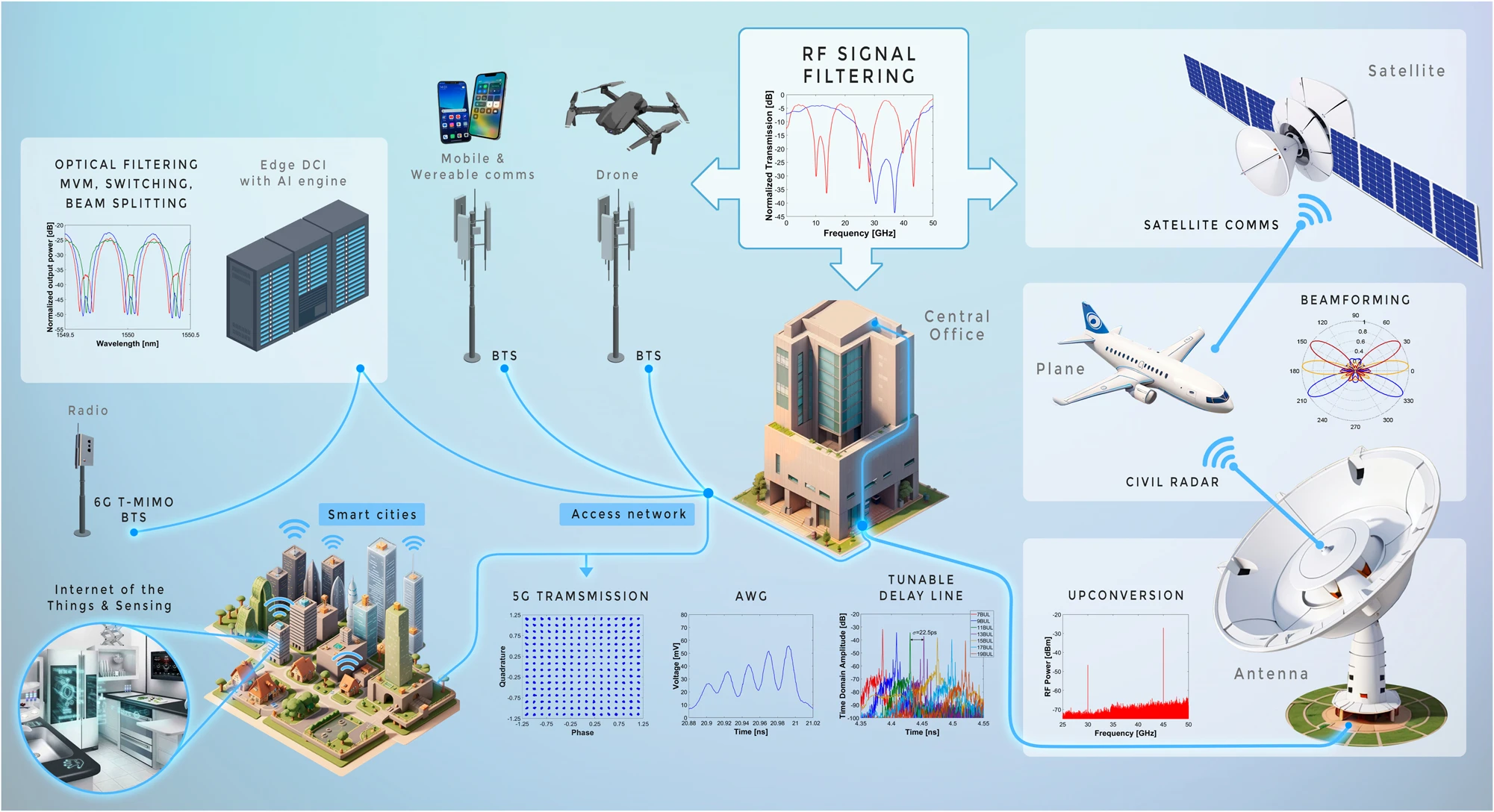
The chip is capable of implementing twelve fundamental functionalities required by certain systems. These functionalities might include tasks like signal modulation, routing, filtering, amplification, and detection, among others. By integrating these functionalities into a single chip, it simplifies the design and implementation of complex optical systems.
One key feature highlighted by Capmany is the chip’s programmability. Unlike fixed-function chips that perform predefined tasks, programmable chips can be configured or reprogrammed to adapt to different requirements. This flexibility allows users to customize the chip’s behavior based on specific applications or changing needs, increasing the efficiency and versatility of the circuit.
“It is the first chip in the world with these characteristics,” said José Capmany, a professor of optical communications at UPV. “It can implement the twelve basic functionalities required by these systems and can be programmed on demand, thus increasing the efficiency of the circuit.”
This innovation is expected to improve technologies like 5G communication, data center efficiency, and artificial intelligence. It also has potential applications in areas like quantum computing, autonomous vehicles, and drones
Read More: TSMC Unveils Silicon Photonics Based Packaging Platform for AI Chips
Industry Impact and Future Prospects:
The integration of this revolutionary chip into iPronics’ Smartlight processor marks a pivotal moment in the advancement of computing technology.
The chip developed by iPronics has been incorporated into one of their products, known as the Smartlight processor, which is currently undergoing testing by Vodafone.
With Vodafone currently testing the Smartlight processor, the commercial viability of the photonic chip is being validated in real-world scenarios. Looking ahead, the scalability of this technology holds immense potential for meeting the evolving needs of data centers and AI computing systems, thereby driving further innovation in the field.
Read the detailed research Paper here
Conclusion:
The development of the world’s first universal, programmable, and multifunctional photonic chip represents a paradigm shift in computing technology. By harnessing the power of light, this groundbreaking innovation promises to unlock new possibilities in telecommunications, data processing, and AI systems. As researchers continue to push the boundaries of photonic computing, the future of technology appears brighter than ever before.