Introduction:
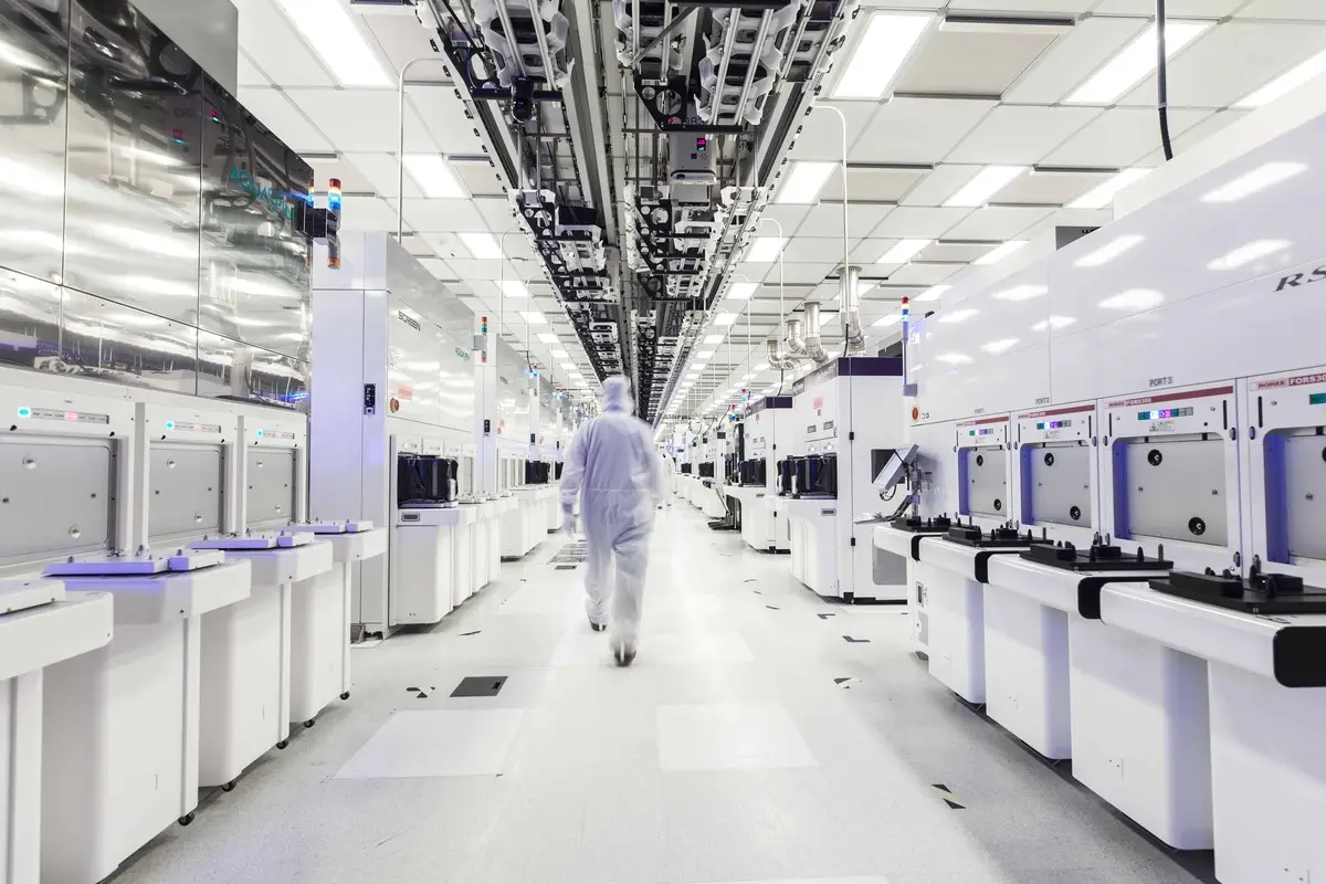
The semiconductor manufacturing industry is at the cusp of a transformative era, witnessing a confluence of technological trends that promise to redefine the landscape in 2024.
In this dynamic environment, nine major trends are set to propel semiconductor manufacturing into new dimensions of performance, efficiency, and versatility.
8 Major Trends in Semiconductor Manufacturing in 2024
1. Sub-2nm Technology: Revolutionizing Transistor Densities
Sub-2nm technology emerges as the vanguard of semiconductor innovation, introducing transistors with a gate pitch as small as 45nm and a metal pitch of 20nm.
Various semiconductor manufacturers are exploring new Front-End-of-Line (FEOL) technologies such as MBCFET, GAAFET, and RibbonFET.
These advancements enable the packing of more transistors onto a single chip, leading to remarkable improvements in overall performance.
Read More: Samsung’s 3 nm Secret: GAA Transistors
2. Vertical Packing: Unleashing the Power of 3D Stacking
The relentless ascent of 3D stacking continues, allowing the stacking of multiple chips to enhance both performance and density.
As the cost of 3D stacking gradually decreases, this technology is becoming more accessible, paving the way for its integration into a broader array of applications, from cutting-edge consumer electronics to critical automotive and medical devices.
Read More: Explained: What the hell is 3D IC packaging?
3. Advanced Materials: Redefining Semiconductor Efficiency
The advent of advanced materials plays a pivotal role in enhancing semiconductor performance and efficiency.
High-k dielectric materials are replacing conventional silicon dioxide in gate insulators.
This shift minimizes leakage current and facilitates the creation of smaller transistor dimensions, contributing to a holistic improvement in semiconductor device performance.
Read More: What is Moore’s Law, More than Moore, and Beyond Moore?
4. Workforce Challenges: Bridging the Skills Gap
The semiconductor industry’s rapid expansion and the demand for sophisticated facilities necessitate a skilled workforce.
The shortage of skilled workers poses a considerable challenge, making it imperative for the industry to invest in training programs and educational initiatives. Addressing this workforce gap is crucial to sustaining the industry’s growth trajectory.
Read More: 85k Jobs but 80% may remained Unfulfilled by 2030 in US Manpower Crisis
5. xUV Lithography: Precision at Sub-2nm Scale
The sub-2nm node is driving the development of cutting-edge lithography equipment, with industry leader ASML at the forefront.
The introduction of 2nm and 1nm EUV lithography machines with high Numerical Aperture (NA) values marks a significant leap forward.
The precision afforded by these machines, with a NA value of 0.55 for 2nm and 1nm models, disrupts conventional semiconductor processing nodes, setting new standards for precision and scale.
Read More: What is EUV that made ASML the biggest company of Europe
6. Chiplets: Revolutionizing SoC Design and Manufacturing
The paradigm of System-on-Chip (SoC) design is evolving with the introduction of chiplets.
Designing with multiple chiplets necessitates managing diverse manufacturing flows and bringing them together seamlessly.
This approach not only offers greater flexibility but also sets new standards for chip designers, driving the development of next-gen application-level system solutions.
Read More: How Chiplets Can Change the Future by extending Moore’s law
7. AI-Driven Solutions: Tackling Complexity at Sub-2nm Level
The increasing complexity of devices at the sub-2nm level necessitates advanced solutions for inspection and diagnosis.
AI-driven solutions are emerging as a powerful tool to navigate this complexity. High-resolution AI solutions accelerate the development process, ensuring high yields, improved performance, and reduced time to market.
EDA tool vendors are leveraging AI to empower chip designers, facilitating a smoother transition between generations.
Read More: 3 Ways Synopsys and Cadence are Using AI in their EDA tools
8. Cost Challenges: Innovating Amidst Margin Pressures
The perpetual increase in semiconductor manufacturing costs poses a challenge, impacting profit margins across the industry.
As costs rise, new manufacturing houses face hurdles in realizing faster returns on investment. Striking a delicate balance between innovation and cost-effectiveness becomes imperative for sustainable growth, requiring a strategic approach to manufacturing processes and resource allocation.
Read More: 2nm Chip Design Costs $725 Million: Can the Industry Afford It?
Conclusion:
In 2024, the semiconductor manufacturing industry stands at the crossroads of unprecedented innovation.
These nine trends collectively promise a future where semiconductor devices are not only faster and more efficient but also adaptive to a wide range of applications.
Navigating this landscape necessitates a harmonious blend of cutting-edge innovation, strategic workforce development, and cost-effective manufacturing practices. The industry’s ability to embrace these trends will shape its continued evolution and success in the years to come.


