Introduction: A Crucial Challenge Unfolds
In the quiet morning hours, within the dimly lit walls of his office, Mark faced a monumental problem that could make or break his career as a photolithography process engineer.
The issue at hand was nothing short of critical: a “Critical Mask Alignment Failure Detected” error had brought the production line to a grinding halt. The stakes?
The destiny of the world’s first highly efficient and ultra-compact microprocessor chip.
The High-Stakes Project: A Glimpse into the Future
This wasn’t just any project; it was a groundbreaking endeavor that promised to redefine the landscape of computing.
A microprocessor chip with unprecedented processing power, compact enough to fit in the palm of a hand, and capable of outperforming even the most advanced supercomputers. The potential was mind-boggling, offering a glimpse into a new era of computing devices.
Also Read: A Day in the Life of a CMP Process Engineer
Revolutionizing Technology: The Quantum Leap
At the heart of this technological marvel was a daring innovation – a chip architecture that harnessed the power of quantum tunneling effects at room temperature.
The concept was ingeniously simple yet astonishingly powerful. The microprocessor chip incorporated a novel architecture that leveraged quantum tunneling effects at room temperature.
This breakthrough allowed for a staggering increase in computational density, enabling millions of intricate calculations to occur simultaneously within a chip that was smaller than a postage stamp.
This ingenious approach allowed for an unparalleled increase in computational density, enabling the execution of millions of intricate calculations simultaneously within a microchip smaller than a postage stamp.
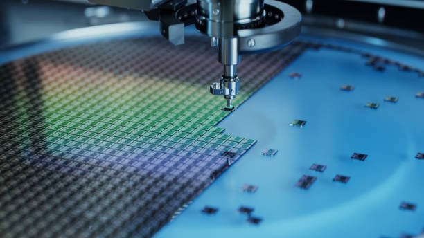
The Critical Hurdle: Mask Alignment Precision
However, the seemingly invincible project had hit a roadblock. The precise arrangement of quantum structures within the chip required immaculate mask alignment during the photolithography process.
Even a minuscule misalignment threatened to compromise the chip’s remarkable capabilities, putting the entire project in jeopardy.
The Emergency Meeting: Seeking Solutions
With the future of computing technology hanging in the balance, Mark assembled his team for an urgent meeting.
Together, they dissected the problem: the mask alignment system was off by a fraction of a micron, causing a cascade of defects and rendering painstaking hours of manufacturing futile.
The challenge was laid bare – a dire situation demanding an innovative solution.
The Unconventional Inspiration: A Ray of Hope
Hours of brainstorming yielded a flicker of hope in the form of an obscure research paper Mark had encountered years ago.
The paper described an audacious approach – using advanced machine learning algorithms and real-time feedback to predict and rectify alignment errors on-the-fly. While a long shot, it was the glimmer of possibility they needed.
No one had used Machine learning to solve a photolithography problem before
Unveiling the Solution: Machine Learning and Real-Time Feedback
The method that Mark and his team decided to implement involved a unique blend of advanced machine learning algorithms and real-time feedback systems, a combination that hadn’t been tried before in the context of photolithography. The process was intricate, but the potential payoff was enormous.
Data Collection and Analysis: The first step was to gather an extensive dataset of past mask alignment errors and corresponding correction actions. This dataset was then used to train machine learning models. The team meticulously categorized each error based on the patterns they exhibited and the corrective measures that were taken.
Machine Learning Model Development: The team developed a set of machine learning algorithms that could process real-time data from the mask alignment system and predict potential alignment errors based on the ongoing process. These algorithms took into account a range of variables, including the lithography equipment’s performance, environmental conditions, and historical alignment patterns.
Real-time Feedback Integration: The next challenge was integrating the machine learning models with the existing mask alignment system. This required developing a feedback loop that continuously monitored the alignment process and fed data to the machine learning algorithms. As the system ran, it collected data on mask-substrate alignment and sent it to the machine learning models for analysis.
Predictive Corrections: The machine learning algorithms, now armed with real-time data, were capable of predicting potential alignment errors before they occurred. When an impending error was detected, the system would automatically initiate corrective measures. These corrections could involve minute adjustments to the mask or substrate positions, compensating for the predicted misalignment.
Adaptation and Learning: One of the most remarkable aspects of this approach was its ability to learn and adapt over time. As the system encountered new alignment scenarios, the machine learning algorithms continuously refined their predictions and corrective actions, improving the accuracy of the entire process with each iteration.
Testing and Fine-Tuning: Before implementing the new system on the production line, the team conducted extensive testing and fine-tuning. They simulated a wide range of alignment scenarios and observed how the system responded. This iterative process helped them optimize the algorithms and ensure reliable performance.
Triumphant Implementation: With the machine learning algorithms integrated and the real-time feedback loop in place, the new alignment system was ready for its first test run on the actual production line. The team held their breath as the process began, watching as the algorithms analyzed incoming data and made predictive corrections in real time.
As the production line hummed along, the new system demonstrated its prowess. Alignment errors that would have previously caused critical failures were now being predicted and corrected on-the-fly.
Mark and his team watched in awe as the chips emerged from the process with near-perfect alignment, a stark contrast to the challenges they had faced earlier.
The implementation of this cutting-edge approach was a game-changer. It not only salvaged the current project, but it also promised to revolutionize photolithography processes across the industry.
Mark’s ingenious solution had turned a dire situation into a resounding success, showcasing the remarkable power of combining advanced technology with creative problem-solving.
The Triumphant Moment: A Future Secured
The culmination of their laborious efforts came to fruition when the production line roared to life once again. Gasps of amazement filled the room as the real-time feedback system sprang into action, aligning the intricate patterns of the mask and substrate with unparalleled precision.
The results were astounding – near-perfect chips, with alignment errors reduced to a fraction of their former magnitude.
Conclusion: A Testimony to Human Ingenuity
Exhausted but exhilarated, Mark returned home, a sense of accomplishment warming his heart. The day had been a true test of skill and creativity, a testament to the remarkable power of human ingenuity.
What began as an insurmountable challenge concluded as a resounding victory, ensuring the future of computing technology was brighter than ever before. As Mark closed his eyes, he knew that this extraordinary journey would forever be etched in the annals of technological history.
The world got its chip & Mark- his sleep!