
Introduction
The world of semiconductor technology is a dynamic and ever-evolving field, where innovation continually pushes the boundaries of what’s possible in terms of performance, miniaturization, and efficiency. In a groundbreaking development, Intel researchers have recently unveiled a 3D monolithic Complementary Field-Effect Transistor (CFET) device that promises to revolutionize the landscape of semiconductor design. This innovative device combines the power of three-dimensional stacking with the complementary operation of n-type and p-type transistors, all while incorporating advanced Atomic Layer Deposition (ALD) technology.
In this blog post, we will delve into the significance of the 3D monolithic CFET device, its key features, and the pivotal role played by ALD technology in its manufacturing.
Join Our WhatsApp News for updated information on semiconductors & AI
Intel 3D Monolithic CFET Device
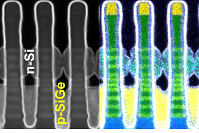
The 3D monolithic CFET device represents a breakthrough in semiconductor design. It’s a fusion of two essential components – three-dimensional stacking and the Complementary Field-Effect Transistor design. This novel approach vertically integrates both n-type and p-type transistors on the same substrate, bringing about several benefits for semiconductor technology.
Key Features:
Denser Circuits: This device excels at producing functional inverters with an impressively small 60 nm gate pitch. This 60 nm gate spacing indicates a highly compact design, enabling the creation of denser circuits. Such miniaturization is crucial for advancing smaller yet more powerful electronic devices.
Vertical Stacking: The device features vertically stacked dual-Source/Drain epitaxy, enhancing space efficiency. Additionally, it utilizes dual metal work function gate stacks. This vertical stacking minimizes interconnect delays and enhances overall efficiency.
Backside Power Delivery: Backside power delivery with direct device contacts significantly contributes to the device’s performance and heat dissipation. This is a crucial innovation for maintaining the optimal operation of electronic devices.
Nanoribbon “Depopulation” Method: Intel researchers introduced a method for varying the number of n-MOS/p-MOS devices in the CFET structure, offering flexibility in tailoring the device to specific applications.
Read More: Micron Unveils NVDRAM: Revolutionary DRAM-Like Non-Volatile Memory for AI

The Role of ALD Technology
At the heart of manufacturing the 3D monolithic CFET device is Atomic Layer Deposition (ALD) technology. ALD plays a pivotal role in crafting the architecture and providing atomically precise and even thin film layers at small scales.
ALD’s Contributions:
Even Coverage: In 3D designs, especially on vertical areas and inside deep gaps, achieving even coverage is challenging but crucial. ALD excels in this aspect, ensuring that every nook and cranny of the device is coated with materials precisely and uniformly.
Transistor Gate Stacks: ALD is used to deposit important materials in transistor gate stacks, including High-k/Metal Gates (HKMG). This is essential for controlling the flow of current and enhancing the transistor’s performance.
Barrier and Seed Layers: Barrier and seed layers are crucial in semiconductor manufacturing. These layers help maintain the integrity of the device and enable the growth of subsequent layers. ALD ensures that these layers are applied accurately, contributing to the overall reliability of the CFET device.
Doping and Spacer Creation: ALD also plays a vital role in doping, which alters the behavior of semiconductors, and in creating spacers that help separate and define different parts of transistors. These techniques are essential for fine-tuning the device’s properties.
Read More: Explained: What the hell is memory?
Conclusion
Intel’s 3D monolithic CFET device, with its 60 nm gate pitch and advanced features, promises to reshape the semiconductor landscape, offering more compact, efficient, and high-performing electronic devices. The integration of ALD technology is instrumental in achieving the precision and uniformity required for such a cutting-edge device.