Introduction:
In the ever-evolving landscape of semiconductor technology, Micron, a leading American memory manufacturer, has announced a groundbreaking initiative to integrate Canon nano- semiconductor printing technology into its DRAM production processes. This strategic move aims to drive down the production costs associated with Dynamic Random Access Memory (DRAM) and enhance the efficiency of Micron’s manufacturing operations.
Follow us on LinkedIn for everything around Semiconductors & AI
Micron Exploration of Canon Nano-Semiconductor Printing:
During a recent presentation, Micron delved into the intricate details of employing nanoscale semiconductor printing for DRAM production.

Image Credits: Semiconductor Engineering
The focus of the discussion included the DRAM fabrication process and the resolution of immersive exposure, specifically highlighting the increasing number of Chop layers.
In semiconductor manufacturing, particularly in processes like DRAM production, a “chop layer” refers to a specific layer within the fabrication process. The term “chop” typically denotes a step or layer where the wafer or substrate is divided into individual units or dies.
Chop layers are crucial because they delineate the boundaries between individual memory cells or other functional units on the semiconductor wafer. These layers help define the size and arrangement of the components on the chip, such as transistors, capacitors, and interconnects.
As the number of Chop layers rises, more exposure steps are required to eliminate false structures surrounding the dense memory array – commonly known as dummy structures.
Challenges in Optical Exposure for DRAM Layers:
Due to the inherent optical characteristics of the system, it becomes challenging to use optical exposure for DRAM layer patterns.
Challenges with Optical Exposure: Optical exposure, a traditional method used in semiconductor manufacturing, faces inherent limitations when applied to DRAM layer patterns. These limitations arise due to the optical characteristics of the system, which may include issues such as resolution limitations, distortion, and difficulty in accurately reproducing intricate patterns.
Refined Approach of Nanoscale Semiconductor Printing: Nanoscale semiconductor printing offers a more refined and precise approach to printing patterns on semiconductor wafers. This technique allows for higher resolution and greater control over the printing process, resulting in more accurate reproduction of complex patterns required for DRAM fabrication.
Cost Efficiency of Nanoscale Semiconductor Printing: Despite the advanced capabilities of nanoscale semiconductor printing, it is reported to be 20% less expensive than traditional optical exposure methods. This cost efficiency makes it an attractive option for semiconductor manufacturers like Micron, as it helps reduce the overall production costs associated with DRAM manufacturing.
Complementary Nature of Nanoscale Semiconductor Printing: It’s essential to understand that nanoscale semiconductor printing does not entirely replace traditional exposure methods in all stages of memory production. Instead, it complements traditional techniques by offering a cost-effective alternative for specific steps in the manufacturing process. By integrating both technologies, semiconductor manufacturers can reduce operational costs while maintaining high-quality standards in DRAM production.
Beyond 1β node, it adopt to huge multi-pattern process for cell array to struct in DRAM scaling. Current exposure technology use multiple patterns in cell array. On the other hand, the lithography process for peripheral circuits use a single exposure, alignment tree become separate for that. However, as scaling progress in the multi-pattern edge cutting process, overlay requirement become tight, requiring high-precision overlay accuracy and control using immersion technology. Current DRAM has a 6F2 structure, pitch of the cell array become narrow by continue to be scaling, also the peripheral contact to M0 must take care of the overlay of the peripheral circuit and cell array. An approach to this problem is to fork-cut the edges of the cell array using nanoimprint(NIL), which double the overlay margin between the peripheral contact and the cell array. In this report, we review nanoimprint cuts applied during the patterning process and discuss the application of edge cut.
~Tomohiro Iwaki, Micron Memory Japan, Inc. (Japan)
Canon Role in Nano-Semiconductor Printing for Micron DRAM
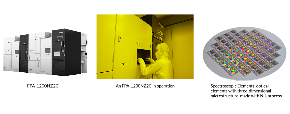
Canon entered the nanoscale semiconductor printing arena with the introduction of the FPA-1200NZ2C Nanoscale Semiconductor Printing (NIL) equipment in October 2023. Fujiwara Fujio, President of Canon, emphasized that the advent of nanoscale semiconductor printing opens up new avenues for small semiconductor manufacturers to produce advanced chips.
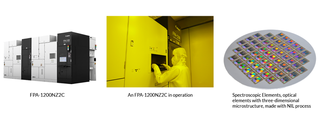
Canon’s Nanoscale Semiconductor Printing involves imprinting the mask with semiconductor circuit patterns onto a wafer. A single imprint can create complex 2D or 3D circuit patterns at the appropriate locations.
With improvements in the mask, Canon’s technology even enables the production of 2-nanometer chips.
SPIE Notification here
Conclusion:
Micron’s collaboration with Canon in integrating nanoscale semiconductor printing into its DRAM production signifies a significant leap towards innovation and cost efficiency in the semiconductor industry.
By combining the strengths of traditional exposure techniques with the precision and cost-effectiveness of nanoscale semiconductor printing, Micron is poised to enhance its competitiveness and contribute to the advancement of memory technologies.
Canon’s pioneering contributions in nanoscale semiconductor printing further underscore the potential of this technology in revolutionizing semiconductor manufacturing, providing new pathways for smaller manufacturers to thrive in the highly competitive semiconductor market.