Introduction:
Semiconductor manufacturing is a dynamic field, constantly evolving to meet the demands of increasingly complex and powerful electronic devices. TSMC, one of the leading semiconductor foundries globally, is on the brink of a major advancement with the upcoming mass production of its performance-optimized 3nm N3P process.
TSMC, a major manufacturer of computer chips, is gearing up for the mass production of their latest chip technology, the 3nm N3P process. Here’s a breakdown of what this means:
Timing: N3P is on track to enter mass production in the second half of 2024.
Performance: This new process offers a refinement of their previous 3nm N3E technology. It boasts both increased performance and improved efficiency.
- Specifically, chip designers can choose to either:
- Increase performance by 4% while maintaining the same power consumption.
- Reduce power consumption by 9% while maintaining the same clock speed (the speed at which a processor executes instructions).
- Density: N3P also packs more transistors into the same space compared to N3E. This translates to potentially more powerful or smaller chips.
This blog post delves into the intricacies of this cutting-edge technology and its implications for the semiconductor industry.
Follow us on LinkedIn for everything around Semiconductors & AI
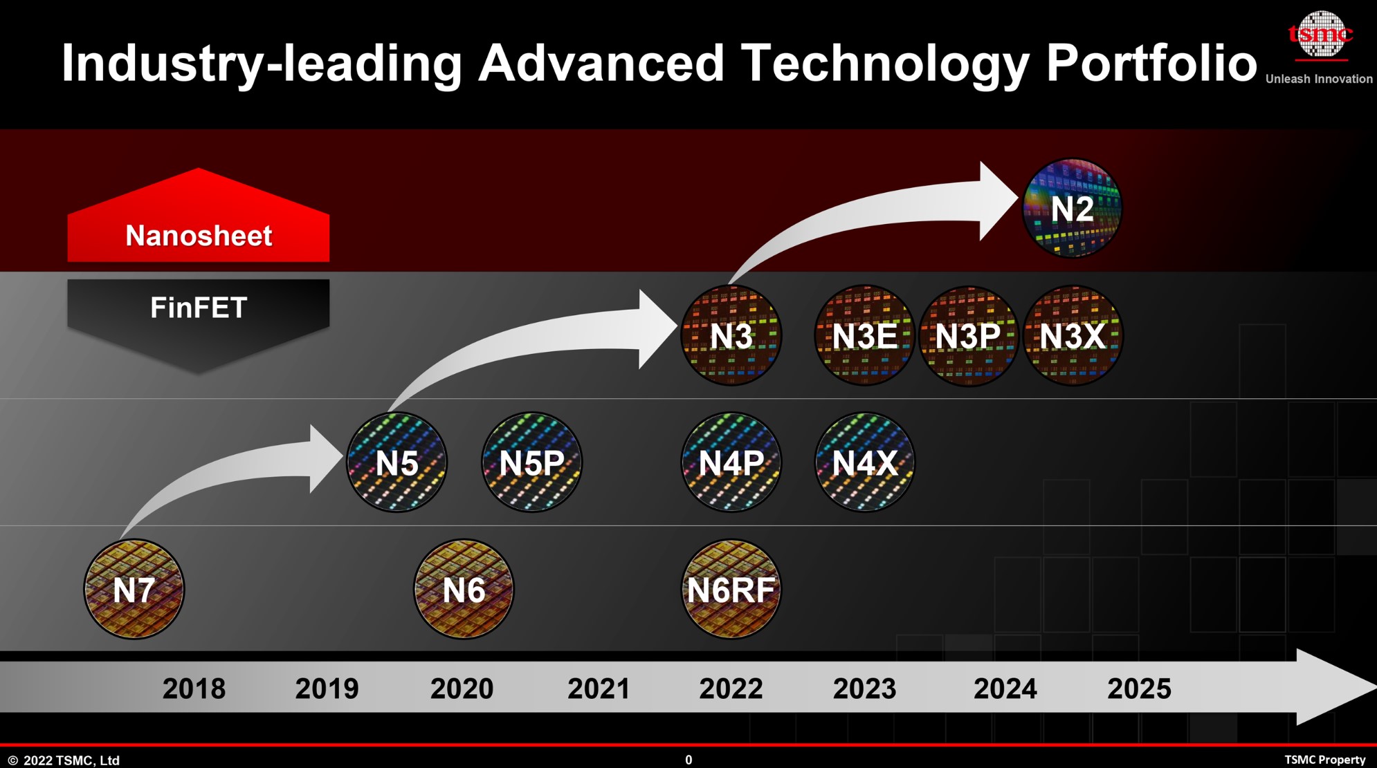
Evolution of Semiconductor Technology
The journey of semiconductor technology has been marked by continuous innovation and miniaturization.
From the early days of large-scale integrated circuits to today’s nanometer-scale processes, the semiconductor industry has made remarkable progress.
TSMC has been at the forefront of this evolution, consistently introducing advanced process nodes to enable the development of faster, more efficient chips.
Introducing the 3nm N3P Process
The 3nm N3P process represents the culmination of years of research and development efforts aimed at pushing the boundaries of semiconductor manufacturing.

Building upon the success of its N3E process, TSMC has fine-tuned the N3P process to optimize performance while maintaining power efficiency.
This optimization involves intricate adjustments to transistor design, materials, and manufacturing techniques to achieve the desired balance between speed and energy consumption.
Technical Improvements: N3P utilizes an “optical shrink” technique. This essentially refines the manufacturing process of N3E, allowing for even smaller transistors to be etched onto the chip. This densification is what unlocks the performance and efficiency gains.
Design Flexibility: The 4% performance improvement or 9% power reduction figures aren’t set in stone. Chip designers have the flexibility to prioritize one over the other based on the specific needs of the product. For instance, a high-performance laptop CPU might prioritize the performance boost, while a battery-powered smartphone chip might focus on power reduction.
Transistor Density Increase: N3P is expected to deliver a 4% increase in transistor density compared to N3E for a “mixed” chip design. This refers to a typical chip layout with logic gates (responsible for computations), SRAM (memory for frequently accessed data), and analog circuits (for interfacing with various components). A higher density allows for more powerful chips in the same size, or smaller chips with similar performance.
Yield Rate: According to TSMC, N3P’s yield rate (the percentage of successfully manufactured chips) is nearing N3E levels. This is important because a high yield rate translates to lower production costs and faster availability of chips for consumers.
Key Features and Benefits
The N3P process boasts several key features and benefits that make it an attractive option for chip designers:
Enhanced Performance Efficiency: By leveraging advanced materials and innovative design techniques, the N3P process enables a 4% increase in performance without sacrificing power efficiency. This improvement allows for faster and more responsive electronic devices, enhancing user experience across a wide range of applications.
Increased Transistor Density: With a 4% boost in transistor density for mixed chip designs, the N3P process enables the integration of more functionality into smaller silicon footprints. This translates to smaller, more power-efficient chips that can deliver higher performance in compact form factors.
Seamless Compatibility: The N3P process facilitates seamless transitions for chip designers. It maintains compatibility with industry-standard EDA tools, IP blocks, and design rules. This compatibility streamlines the development process. It ensures that designers can leverage existing methodologies and toolsets effectively. Overall, N3P reduces the time-to-market for innovative semiconductor solutions.This streamlines development, reducing time-to-market for innovative semiconductor solutions.
Industry Implications and Applications
The impending mass production of the N3P process holds far-reaching implications for various industries and applications:
- Mobile Devices: Smartphones, tablets, and wearables stand to benefit from the enhanced performance and power efficiency offered by the N3P process. These devices can deliver smoother multitasking, faster app launches, and longer battery life, enhancing user productivity and satisfaction.
- Data Centers: The N3P process’s combination of performance and energy efficiency makes it an ideal choice for data center applications. From high-performance computing to artificial intelligence and machine learning workloads, data centers can leverage the N3P process to achieve optimal performance while minimizing operational costs.
- Automotive Electronics: As vehicles become increasingly electrified and connected, the demand for advanced semiconductor solutions continues to rise. The N3P process’s ability to deliver high performance in harsh automotive environments makes it well-suited for applications such as advanced driver assistance systems (ADAS), infotainment systems, and vehicle electrification components.
Looking Ahead
TSMC’s N3P process heralds a new era of technological advancement in the semiconductor industry.
Chip designers worldwide eagerly await its mass production. N3P-based chips offer unparalleled performance, efficiency, and functionality.
TSMC’s track record ensures it remains at the forefront of electronics evolution.
Conclusion:
The impending mass production of TSMC’s performance-optimized 3nm N3P process represents a significant milestone in semiconductor manufacturing.
The N3P process offers enhanced performance efficiency and increased transistor density. It ensures seamless compatibility for chip designers.
This sets the stage for a new era of innovation in electronic devices. TSMC’s commitment to pushing semiconductor technology limits underscores its leadership in shaping the future of technology.