Introduction:
The semiconductor industry stands as a testament to human ingenuity, continually pushing the boundaries of what’s possible in electronics and computing. At the heart of this innovation are patents—legal protections that recognize and reward groundbreaking discoveries and inventions. Throughout history, several patents have left an indelible mark on the semiconductor landscape, shaping the way we live, work, and communicate. In this article, we delve into the top 10 patents that have significantly impacted the semiconductor industry. From the foundational planar transistor to cutting-edge FinFET technology, each patent represents a milestone in the evolution of semiconductor devices.
We’ll explore the problems these patents addressed, how they revolutionized semiconductor technology, and their lasting impact on the world of electronics.
Read More: €3.4 Billion in Government Support: Did China Just Supercharge BYD – techovedas
Read part 1 here
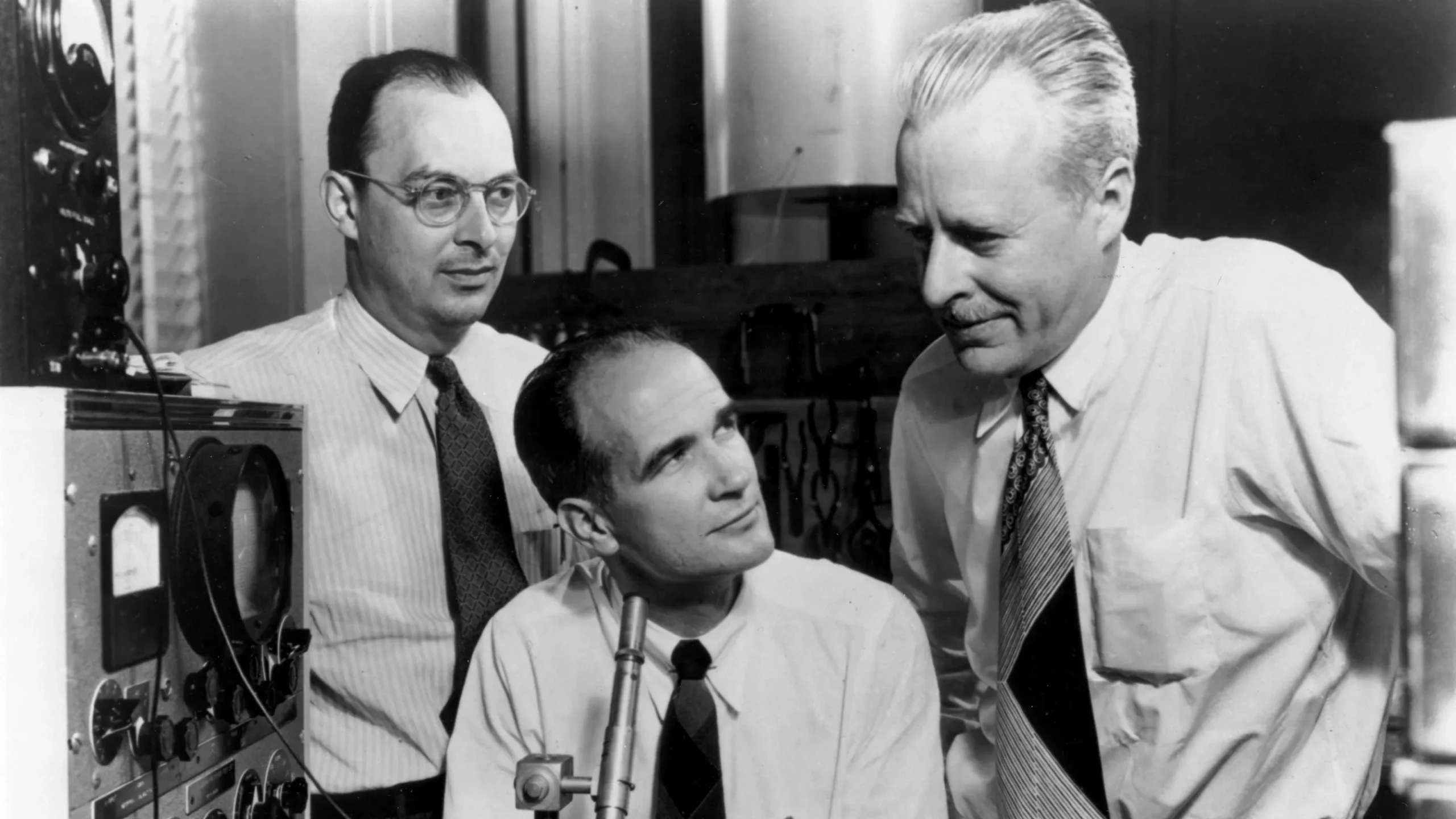
6. Self-aligned Gate process (US Patent 4,413,062) – 1984, by Toshiro Horiuchi and Hisashi Nakamura at Hitachi:
Problem that was being faced:
Fabricating MOS transistors with precise alignment of the gate electrode and source/drain regions was challenging and limited transistor performance and manufacturability.
How did the patent solve this problem?
Toshiro Horiuchi and Hisashi Nakamura’s invention of the self-aligned gate process simplified the fabrication of MOS transistors. It is used by the gate electrode itself to define the source and drain regions. This innovation reduced manufacturing complexity and improved transistor performance.
What was the impact?
The self-aligned gate process revolutionized MOS transistor fabrication by enabling higher transistor densities, improved performance, and reduced manufacturing costs. This contributed to the development of more advanced integrated circuits with increased functionality and performance. Horiuchi and Nakamura’s patent remains a fundamental technology in semiconductor manufacturing.
Read More: 13 Semiconductor Terms Everyone MUST Know
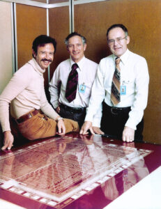
7. Tungsten Metallization (US Patent 4,639,307) – 1987, by Robert Havemann and James McPherson at IBM:
Problem that was being faced:
Metallization layers in integrated circuits faced challenges related to conductivity, reliability, and manufacturability, limiting further advancements in semiconductor technology.
How did the patent solve this problem?
Robert Havemann and James McPherson’s invention of tungsten metallization provided a superior alternative to aluminum for use as a metallization layer in integrated circuits. Tungsten offered higher conductivity and better resistance to electromigration, improving the reliability and performance of ICs.
What was the impact?
The adoption of tungsten metallization significantly enhanced the reliability and performance of integrated circuits. It enabled the production of ICs with smaller feature sizes and higher operating speeds, contributing to advancements in computing and telecommunications. Havemann and McPherson’s patent played a crucial role in the evolution of semiconductor technology, particularly in improving the reliability and manufacturability of integrated circuits.
Read More: What is CMOS 2.0 Revolution: A Paradigm Shift in Chip Design – techovedas
8. Copper Interconnects (US Patent 5,663,077) – 1997, by Richard Fair and Robert Haken at IBM:
Problem that was being faced:
Traditional aluminum interconnects in integrated circuits faced limitations in terms of resistivity and electromigration, which became increasingly significant as transistor sizes continued to shrink.
How did the patent solve this problem?
Richard Fair and Robert Haken’s invention of copper interconnects provided a solution to the limitations of aluminum interconnects by offering lower resistivity and better resistance to electromigration. Copper’s superior conductivity made it ideal for use in high-performance integrated circuits.
What was the impact?
The adoption of copper interconnects revolutionized integrated circuit interconnection technology, enabling faster and more reliable communication between transistors. This resulted in improved performance and reduced power consumption in electronic devices, ranging from microprocessors to memory chips. Fair and Haken’s patent played a pivotal role in advancing semiconductor technology and driving the development of high-performance integrated circuits.
Read More: 10 Patents Which Revolutionized the Semiconductor Industry (Part 1) – techovedas
9. High-k Dielectric Materials (US Patent 6,107,041) – 2000, by Walid Dabbous et al. at IBM:
Problem that was being faced:
Traditional silicon dioxide gate oxides in transistors faced limitations in terms of gate leakage current, which became increasingly problematic as transistor sizes continued to shrink.
How did the patent solve this problem?
Walid Dabbous et al.’s invention of high-k dielectric materials provided a solution to the limitations of silicon dioxide gate oxides by offering reduced gate leakage current. High-k dielectrics allowed for the continued scaling of transistor dimensions while maintaining performance and power efficiency.
What was the impact?
The adoption of high-k dielectric materials revolutionized transistor technology by enabling further miniaturization and improved performance in integrated circuits. This led to the development of more energy-efficient and high-performance electronic devices, including smartphones, tablets, and wearable technology. Dabbous et al.’s patent played a significant role in advancing semiconductor technology and facilitating the transition to smaller and more power-efficient transistors.
Read More: Apple to Invest Over $250 Million in Expanding Singapore Campus – techovedas
10. FinFET (Fin Field-Effect Transistor) (US Patent 6,114,664) – 2000, by Douglas B. Dewey et al. at IBM:
Problem that was being faced:
Traditional planar transistors faced challenges related to gate leakage current and short-channel effects as transistor sizes continued to shrink.
How did the patent solve this problem?
Douglas B. Dewey et al.’s invention of the FinFET introduced a three-dimensional gate structure that offered improved control over gate leakage current and short-channel effects. The fin-shaped structure of FinFETs provided better electrostatic control over the channel, allowing for continued scaling of transistor dimensions.
What was the impact?
The adoption of FinFET technology revolutionized transistor design and enabled further scaling of transistor dimensions beyond the limits of traditional planar transistors. FinFETs became the foundation of modern semiconductor technology, driving advancements in performance, power efficiency, and integration density in integrated circuits. Dewey et al.’s patent played a pivotal role in shaping the future of semiconductor technology and facilitating the development of smaller, faster, and more energy-efficient electronic devices.
Follow us on Linkedin for everything around Semiconductors & AI
Conclusion:
Innovation in the semiconductor industry is a story of perseverance, creativity, and collaboration. The patents highlighted in this article have played pivotal roles in driving technological semiconductor industry progress and shaping the modern world. From the early days of transistor miniaturization to the latest advancements in three-dimensional transistor structures, these inventions have paved the way for smaller, faster, and more energy-efficient electronic devices.
As we look to the future, the spirit of innovation embodied by these patents will continue to propel the semiconductor industry forward. New challenges will emerge, and new solutions will be devised, driving further advancements in electronics, computing, and beyond. By recognizing the significance of these patents, we gain a deeper appreciation for the ingenuity and dedication that have fueled the semiconductor revolution—and inspire the next generation of inventors to push the boundaries of what’s possible.