Introduction
Imagine the evolution of semiconductor technology as a skyscraper being built floor by floor. Initially, we used basic building materials and simple construction methods, but now, Samsung is about to unveil a revolutionary approach akin to advanced skyscraper engineering. By stacking each floor with precision and innovation, they are reaching new heights in efficiency and performance. This is the essence of Samsung’s upcoming “SAINT” 3D packaging services, set to launch in 2025, aimed at next-gen HBM4 memory production.
Follow us on Linkedin for everything around Semiconductors & AI
Background: The Shift from 2.5D to 3D Packaging
The semiconductor industry has seen remarkable advancements, but the transition from 2.5D to 3D packaging marks a significant leap.
Traditionally, 2.5D packaging utilized a silicon interposer to connect High Bandwidth Memory (HBM) and GPUs.
While effective, this method has limitations in speed and efficiency. Enter Samsung’s SAINT (Samsung Advanced Interconnect Technology) platform, which aims to revolutionize this process by focusing on vertical integration, stacking chiplets on top of each other.
What is the Matter?
Samsung is poised to launch its “SAINT” 3D packaging services by 2025, targeting the forthcoming HBM4 memory standard expected to debut in 2026.
This strategic move aims to bolster Samsung’s position in the AI and semiconductor industry, offering significant performance and efficiency improvements.
Cutting-Edge SAINT 3D Packaging Technology
Samsung’s “SAINT” 3D packaging services represent a monumental shift from traditional 2.5D methods.
Unlike the conventional approach, which uses a silicon interposer to link HBM and GPUs, SAINT emphasizes vertical stacking.
This method significantly reduces the distance between chiplets, enhancing data transfer speeds and overall performance.
Increased Performance:
Reduced Distance, Faster Data Transfer: Traditionally, chips are placed side-by-side. SAINT’s vertical stacking brings components physically closer, significantly reducing the distance data needs to travel. This translates to faster communication between memory and processing units, leading to a performance boost.
High Bandwidth with HBM4: HBM4 memory itself is a high-bandwidth solution compared to traditional DRAM. Combining it with the close proximity achieved by 3D stacking allows for even faster data flow, crucial for data-intensive applications like artificial intelligence (AI) and high-performance computing (HPC).
Smaller Footprint:
Vertical Stacking Saves Space: By stacking chips instead of placing them side-by-side, the overall footprint of the chip package is reduced. This allows for designing more compact devices while maintaining high processing power.
Potential Environmental Benefits:
Reduced Materials: Smaller chip packages potentially require less material, leading to a potentially lower environmental impact.
Competitive Landscape:
Positioning for the Future: The development of HBM4 memory and advanced packaging like SAINT positions Samsung as a leader in next-generation chip technology. This could give them an edge in the highly competitive semiconductor market.
Overall, SAINT with HBM4 represents a significant leap in chip packaging technology, promising significant performance improvements and paving the way for smaller, more efficient devices in the future.
Read More: Nvidia to Challenge Intel with Arm-Based PC Chips – techovedas
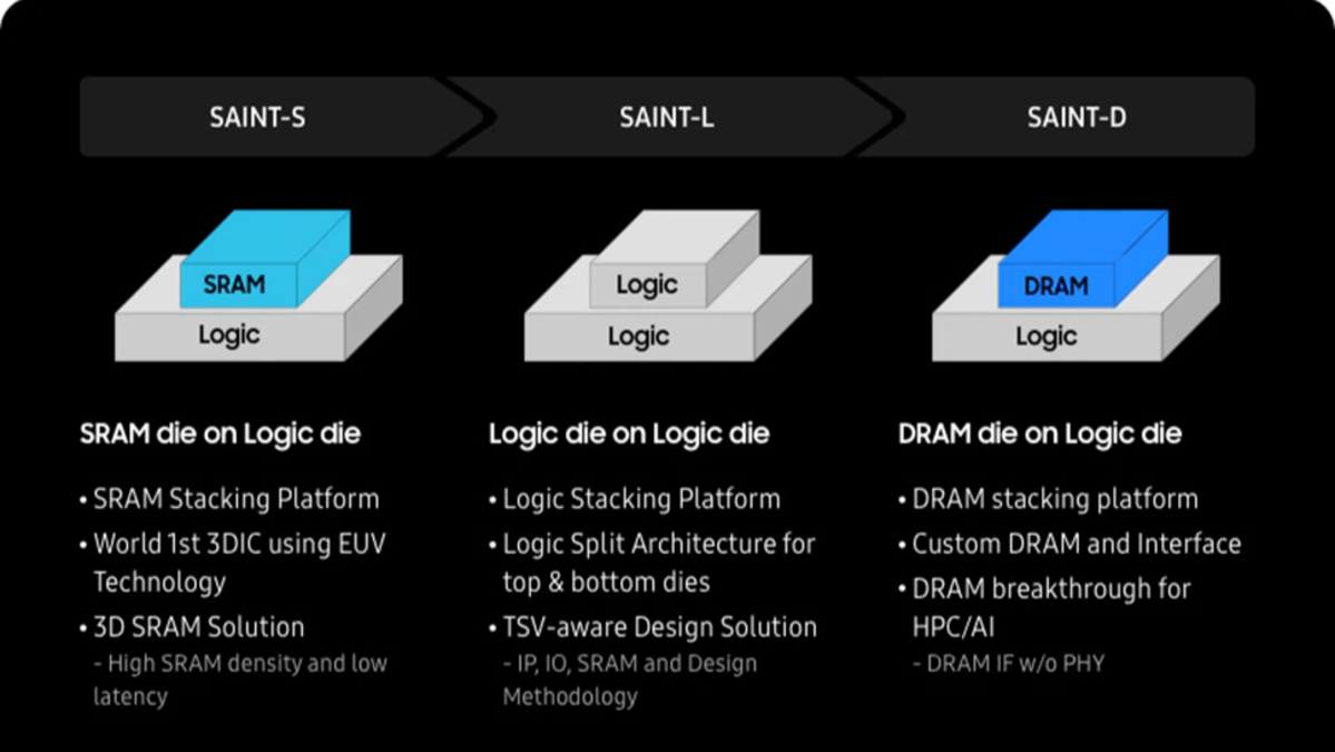
Types of SAINT Packaging
The SAINT platform is categorized into three types, each tailored to specific semiconductor needs:
:
Image Credits: Samsung
- SAINT-S: Designed for SRAM chips.
- SAINT-L: Targeted at Logic chips.
- SAINT-D: Focused on DRAM chips.
Advantages of Vertical Stacking
Vertical stacking offers numerous benefits over 2.5D methods.
By decreasing the distance between chiplets, Samsung’s 3D packaging technology improves data transfer speeds and reduces latency.
Additionally, this approach lowers the carbon footprint, making it an environmentally sustainable option.
These advancements are critical as the demand for high-performance AI hardware continues to rise.
Debut at Samsung Foundry Forum 2024
Samsung showcased its 3D packaging technology at the Samsung Foundry Forum 2024 in San Jose, California.
This public introduction aligns with next-gen announcements from NVIDIA and AMD regarding their AI hardware.
The SAINT platform is expected to be integral to the production of NVIDIA’s Rubin architecture and AMD’s Instinct MI400 AI accelerators, set to debut alongside HBM4 memory by 2026.
Read More:ASICs vs. FPGAs: Choosing the Right Technology for Your Design – techovedas
Future Prospects and Industry Impact
Looking forward, Samsung plans to introduce an “all-in-one heterogeneous integration technology by 2027.
This innovation will unify AI package integration, eliminating the need for separate packaging techniques.
Such advancements position Samsung as a leader in the semiconductor industry, competing with tech giants like Apple and Intel.
Apple and Intel have been pioneers in SOC-centric designs for their thin and light devices, such as Intel’s Lunar Lake CPUs. AMD has also been active in vertical stacking, utilizing HBM, MCD, and 3D V-Cache stacks across multiple chips for both consumers and clients.
Samsung’s advancements in 3D packaging technology are expected to further solidify its competitive position in this rapidly evolving market.
Read More: Air Liquide Commits $250 Million Investment to U.S. Semiconductor Industry – techovedas
Conclusion
Samsung’s forthcoming launch of the SAINT 3D packaging services signifies a groundbreaking advancement in the semiconductor industry.
By introducing this innovative platform, Samsung is set to lead the AI hardware market, offering enhanced performance, efficiency, and sustainability.
As the industry anticipates the debut of HBM4 memory and the integration of cutting-edge AI hardware, Samsung’s strategic innovations will undoubtedly shape the future of semiconductor technology.