Introduction
“Heterogeneous integration” in the context of integrated chips refers to the incorporation of different types of semiconductor components, technologies, or materials onto a single chip or package. This approach contrasts with traditional homogeneous integration, where similar components are integrated using a uniform technology.
In heterogeneous integration, diverse elements such as transistors, memory cells, sensors, and other functional blocks can be combined on the same chip, even if they are manufactured using different processes or materials. This allows for the optimization of each component based on its specific requirements, rather than using a one-size-fits-all approach. Heterogeneous integration is often used to address the limitations of scaling traditional semiconductor technologies and to achieve improvements in performance, power efficiency, and functionality.
Heterogenous is the opposite of homogenous. You must have studied homogenous mixtures in your secondary school. While homogenous means having elements of similar kind, heterogenous involves two or more elements which are of different type and not necessarily complementary.
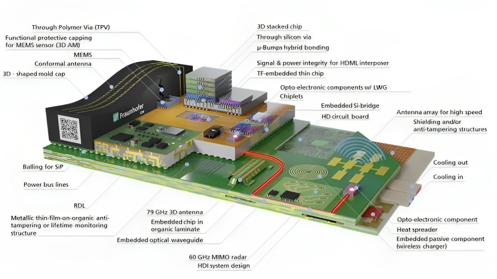
Figure 1. High end performance and heterogenous packaging
Why do we need heterogenous integration?
Moore’s Law fundamentally posits the doubling of transistor density on an integrated circuit (IC) every two years. The integration density of transistors faces limitations in the 2D realm, primarily stemming from the deceleration in the reduction of gate lengths.
Heterogeneous integration is driven by several factors, and it addresses a range of challenges and limitations associated with traditional homogeneous integration. Here are some reasons why heterogeneous integration is important:
Diverse Functionalities:
Different types of semiconductor components excel at specific functionalities. For example, specialized processors, memory elements, sensors, and communication modules may each have unique characteristics optimized for their intended purpose. Heterogeneous integration allows the combination of these diverse elements on a single chip, enabling the creation of more versatile and capable devices.
Performance Optimization:
Heterogeneous integration enables the use of the most suitable technology for each component. This can lead to performance improvements in terms of speed, power efficiency, and overall functionality. By optimizing each functional block independently, designers can achieve better overall system performance.
Moore’s Law Challenges:
As semiconductor technology advances, traditional scaling is becoming increasingly difficult and costly. Heterogeneous integration provides an alternative path for improving performance and functionality without relying solely on shrinking transistor sizes.
Form Factor and Size Reduction:
By integrating different components more closely and efficiently, heterogeneous integration can contribute to reducing the overall size and form factor of devices. This is particularly important in applications where space is constrained, such as in mobile devices or wearable electronics.
Cost Efficiency:
Heterogeneous integration can lead to cost savings by allowing the use of the most cost-effective technology for each component. This is in contrast to homogeneous integration, where a single technology must be applied uniformly across the entire chip.
Addressing Technology Gaps:
Different semiconductor technologies may have varying strengths and weaknesses. Heterogeneous integration provides a way to combine the advantages of multiple technologies, bridging gaps and overcoming limitations to create more robust and advanced systems.
Increased Functionality:
The combination of diverse components on a single chip enables the creation of more sophisticated and feature-rich devices. This is particularly important in applications such as artificial intelligence, where specialized processing units for tasks like machine learning can be integrated alongside traditional components.
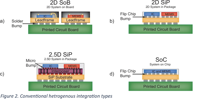
Read More: What is 2D, 2.5D & 3D Packaging of Integrated Chips?
Types of heterogeneous integration
To overcome this constraint, we are employing heterogenous integration of multiple chips of same/different functionality through stacking them on top of each other. This is one type of heterogenous integration.
Another instance is that of smart systems being integrated into various conventional devices. Smart thermostats are available in the market which provide automatic temperature control, a timer and edge AI which learns the usage pattern of the customer. Making such a system heavily employs heterogenous integration of sensors, processors, data storage units and the conventional thermostat.
3D IC (Integrated Circuit):
Stacking multiple layers of integrated circuits vertically to enhance performance, reduce interconnect lengths, and enable more efficient use of space.
Multi-Chip Module (MCM):
Integrating multiple chips into a single module, often on a shared substrate, to achieve compactness and efficient communication between components.
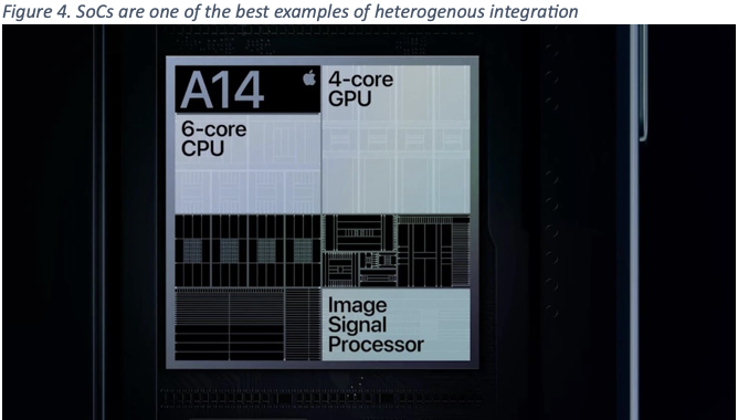
System on Chip (SoC):
A System-on-Chip (SoC) is a semiconductor device that integrates multiple electronic components, such as processors, memory, input/output interfaces, and sometimes specialized components like GPUs or accelerators, onto a single chip. The best example here is Apple’s A14 Bionic chip. It integrated the CPU, GPU, memory into a single chip.
System-in-Package (SiP):
In the 1980s SiPs were available in the form of multi-chip modules. A system in package, or SiP, is a way of building two or more ICs inside a single package. Package here refers to the outer most wrapper of a semiconductor IC. It finds great application in MEMS (discussed ahead).
Wafer-Level Integration (WLI):
WLI is a broader term that refers to integrating various components at the wafer level before the chips are diced and packaged. This can include different technologies and functionalities combined on the same wafer before subsequent processing steps. It encompasses approaches like Fan-Out Wafer Level Packaging (FOWLP) which we will discuss later in this article.
Read More: Explained: What the hell is 3D IC packaging?
Difference between SiP & SoC
System-in-Package (SiP) and System-on-Chip (SoC) are both approaches to integrated circuit design, but they differ in their structure and the level of integration they achieve. Here are the key differences between SiP and SoC:
System-in-Package (SiP):
Definition:
- SiP: SiP refers to a package that contains multiple integrated circuits (ICs) or dies, each performing a specific function. These ICs are combined in a single package, and they may be heterogeneous, meaning they can be manufactured using different technologies.
Integration Level:
- SiP: SiP achieves a high level of integration at the package level but does not integrate all functions on a single silicon die. Different components or chips are packaged together, and they communicate through interconnects within the package.
Flexibility:
- SiP: SiP offers greater flexibility in terms of incorporating diverse components, technologies, and functionalities. It allows for the combination of specialized chips optimized for specific tasks.
Interconnects:
- SiP: Interconnects between the various components are typically established through wire bonding, flip-chip bonding, or other packaging technologies. These interconnects are critical for communication between the different parts of the package.
Advantages:
- SiP: SiP is advantageous when it is not feasible or cost-effective to integrate all functions onto a single chip. It allows for the combination of existing chips or dies, making it suitable for applications where diverse functionalities are required.
System-on-Chip (SoC):
Definition:
- SoC: SoC refers to a single integrated circuit that integrates all or most of the components and functionalities required for a complete electronic system. It typically includes processors, memory, input/output interfaces, and other necessary components on a single silicon die.
Integration Level:
- SoC: SoC achieves the highest level of integration, incorporating multiple functions and components onto a single chip. The goal is to create a self-contained and highly integrated electronic system on a single piece of silicon.
Design Complexity:
- SoC: Designing an SoC involves addressing the challenges of integrating diverse components and functionalities, often requiring advanced semiconductor manufacturing technologies.
Interconnects:
- SoC: Interconnects within an SoC are typically implemented using on-chip wiring and routing. The integration is at the silicon level, with components sharing the same substrate.
Advantages:
- SoC: SoC is advantageous in terms of reduced power consumption, improved performance, and smaller form factor. It is often used in applications where high levels of integration and miniaturization are crucial, such as in mobile devices and IoT devices.
In summary, while both SiP and SoC involve integrating multiple components into a single package or chip, the key distinction lies in the level of integration and where that integration occurs. SiP integrates at the package level, allowing for flexibility in combining different components, while SoC achieves the highest level of integration by incorporating all functions onto a single silicon die.
Read More: Intel to Build First Overseas 3D Chip Packaging Facility in Malaysia
Key Technologies in Heterogeneous Integration
A. Advanced Packaging Techniques
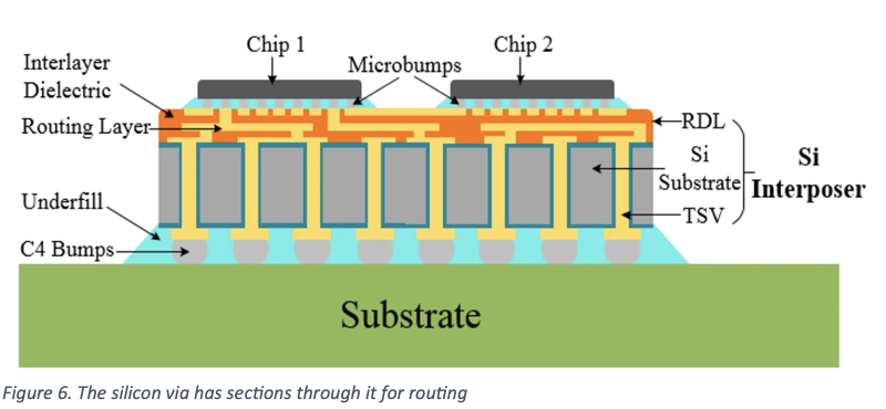
Interposer Technology:
An interposer is a multi-layer printed circuit board (PCB) that acts as a bridge between different chips and components. It provides high-speed data transmission and reduces signal latency by providing shorter interconnect paths compared to traditional packaging methods.
Through-Silicon Via (TSV)
Through-silicon vias (TSVs) are tiny vertical connections that pass through the layers of a silicon wafer, enabling electrical connections between different layers. TSVs provide shorter interconnect paths and higher bandwidth compared to traditional wire bonding techniques, enhancing system performance and reducing signal loss. Particularly used in 3D IC design
Fan-Out Wafer Level Packaging (FOWLP):
FOWLP is a packaging technology that involves redistributing individual chips or components across the surface of a wafer before encapsulation. This redistribution is done without the need for a traditional substrate. FOWLP offers advantages in terms of form factor, cost, and flexibility in design. It enables heterogeneous integration by placing different components on the same package.
B. Integration of Different Materials
Silicon Integration with III-V Materials – Silicon (Si) is the dominant material for CMOS transistors, the workhorse of modern electronic devices. However, group III-V materials of the periodic table, such as gallium arsenide (GaAs) and indium phosphide (InP), offer superior properties for certain applications, particularly in the realm of optics and high-frequency electronics.
Integration of MEMS and Sensors – Micro-Electro-Mechanical Systems (MEMS) and sensors are often integrated into systems using heterogeneous integration. This involves the use of packaging technology to integrate dissimilar chips, photonic devices, or components with different materials and functions4. Examples of 2D approaches include through-silicon via (TSV) interposer, embedded silicon bridge (EMIB)
Future of Heterogenous integration: Growing demand
New packaging techniques, interconnect technologies like TSV, and design tools are emerging to enable more complex and efficient HI solutions.
This demand for HI is driven by the increasing performance requirements of modern electronic systems, particularly in areas such as artificial intelligence (AI), High-performance computing (HPC) and data centres. These applications require heavy compute power and dense integration of heterogenous modules like processor and memory necessary for enhancing performance.