Introduction:
The landscape of high bandwidth memory (HBM) technology is about to undergo a transformative shift with the introduction of SK Hynix groundbreaking 16-layer HBM3E chip.
Scheduled to be unveiled at the prestigious International Society of Solid State Circuits (ISSCC) 2024 conference, this technological marvel promises to redefine the boundaries of data processing speed and capacity in the semiconductor industry.
Follow us on LinkedIn for everything around Semiconductors & AI
The Breakthrough:
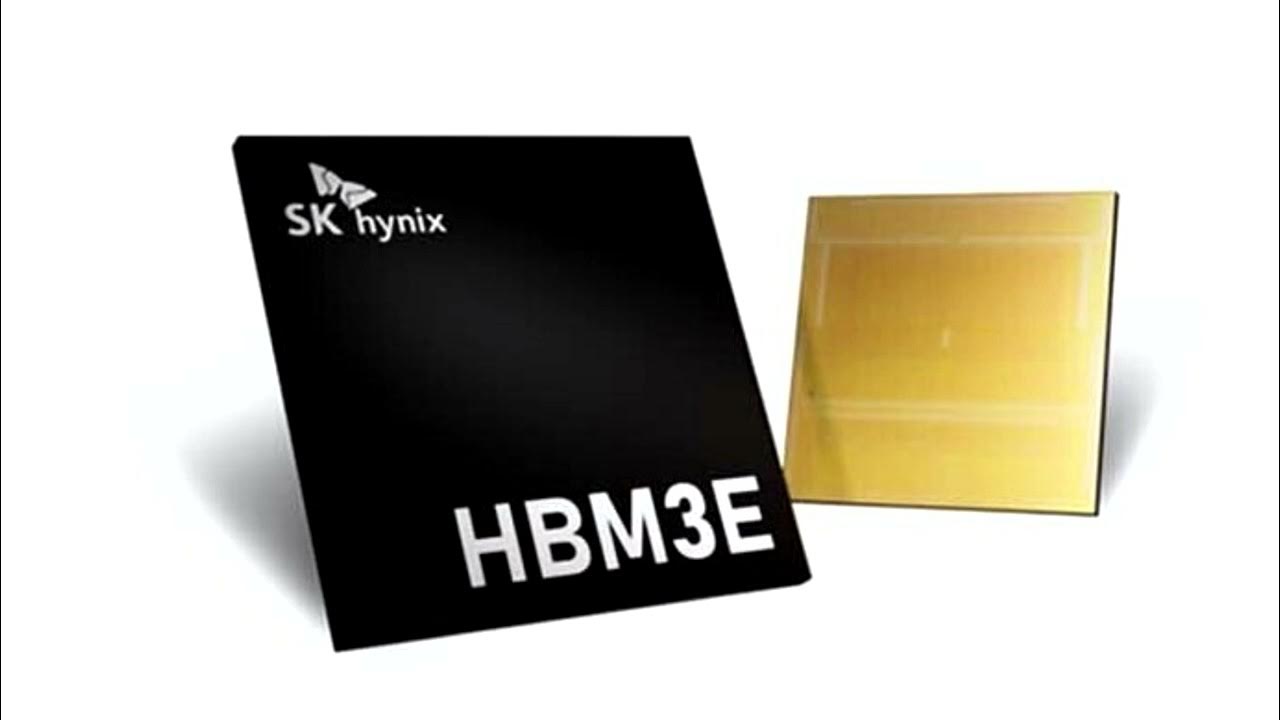
At the heart of SK Hynix’s presentation lies the 16-layer HBM3E chip. It’s a testament to the company’s relentless pursuit of technological advancement.
Boasting an impressive capacity of 48 gigabytes (GB), it sets a new standard. Its unprecedented processing speed of 1280 GB/s per stack is remarkable. This revolutionary chip represents a significant leap forward in HBM technology.
A 16-layer HBM3E is a high-performance type of computer memory. This is designed for use in advanced applications like artificial intelligence (AI) and high-performance computing (HPC). Here’s a breakdown of the key terms:
- 16-layer: This refers to the number of individual memory chip layers stacked on top of each other in a single unit. More layers allow for higher memory capacity.
- HBM3E: HBM stands for High Bandwidth Memory, and 3E indicates the third generation with additional enhancements (E).
Here are some key features of 16-layer HBM3E:
- High Bandwidth: Compared to traditional DDR memory, HBM3E offers significantly higher bandwidth, allowing for faster data transfer between the memory and the processor.
- Large Capacity: A 16-layer HBM3E stack can offer up to 48GB of memory, making it suitable for data-intensive applications.
- Low Power Consumption: SK Hynix, a major manufacturer of HBM, claims that their 16-layer design optimizes power efficiency through Through-Silicon Via (TSV) technology.
Overall, 16-layer HBM3E represents the cutting edge of memory technology, offering significant advantages in bandwidth, capacity, and potentially lower power usage compared to previous generations.
- SK Hynix is a frontrunner in HBM3E technology, showcasing a 16-layer stack at the 2024 International Solid-State Circuits Conference (ISSCC 2024). They had previously offered samples of 12-layer HBM3E in 2023.
- While 16-layer HBM3E is a significant advancement, research and development are ongoing for even higher performing memory solutions like 16-layer HBM4, expected for mass production by 2026.
Read More: Samsung vs. SK Hynix in the Battle for HBM Dominance – techovedas
The development of the 16-layer HBM3E chip presented several technical challenges. This includes the need for thinner DRAM dies and the prevention of wafer warpage during the stacking process.
To overcome these obstacles, SK Hynix leveraged advanced MR-MUF (Mass Reflow Molded Underfill) technology. This enhances heat dissipation performance while minimizing package size.
Read More: Why AI Needs a New Chip Architecture – techovedas
The Event:
Taking center stage at the ISSCC 2024 conference in San Francisco, USA, SK Hynix will showcase its unparalleled expertise in semiconductor design and manufacturing.
With over 3,000 semiconductor engineers from around the world in attendance, ISSCC earns renown as the “Olympics of semiconductor integrated circuit design technology.”
This prestigious event offers the ideal platform for SK Hynix to showcase its latest innovation to a global audience of industry experts, fostering collaboration and driving technological advancement in the semiconductor field.
Market Outlook:
The increasing adoption of artificial intelligence (AI) and other data-intensive applications fuels the growth of the market.
Market research forecasts robust growth in the HBM market. SK Hynix and its competitors are well-positioned to capitalize on this trend.
Conclusion:
SK Hynix unveiling of the 16-layer HBM3E chip marks a significant milestone in the evolution of high bandwidth memory technology.
This groundbreaking chip sets a new standard for data processing speed and capacity. It reaffirms SK Hynix’s position as a pioneer in the semiconductor industry.
The demand for high bandwidth memory continues to grow. SK Hynix remains committed to pushing the boundaries of innovation. It delivers cutting-edge solutions to meet the evolving needs of the market.