Introduction:
TSMC, one of the leading semiconductor manufacturers, has unveiled groundbreaking advancements in wafer-scale computing technology. This innovative approach promises to revolutionize the landscape of computing, offering unprecedented levels of performance and scalability. From the current iteration to the anticipated advancements by 2027, TSMC’s journey into wafer-scale computing holds immense potential for the future of technology.
Follow us on Linkedin for everything around Semiconductors & AI
Background:
The semiconductor industry has long relied on Moore’s Law, which posits that the number of transistors on a microchip double approximately every two years, to drive advancements in computing power.
However, as transistor sizes approach physical limits, traditional scaling methods have become increasingly challenging.
In response, TSMC has pioneered wafer-scale integration, a novel approach that promises to overcome the limitations of traditional scaling and unlock new levels of performance.
Read More:$545 Million: Shin-Etsu to Invest in Lithography Material Plant in Japan – techovedas
Current State of Wafer-Scale Computing:
Traditionally, the semiconductor industry has relied on scaling down the size of transistors to enhance computing power.

However, as this approach approaches its physical limits, TSMC has introduced wafer-scale integration as a transformative solution.
The current iteration of TSMC’s wafer-scale technology enables the creation of large-scale computing systems using multiple dies on a single wafer.
Read More:$545 Million: Shin-Etsu to Invest in Lithography Material Plant in Japan – techovedas
TSMC Roadmap for Wafer Scale Technolgy Roadmap
Here’s what we know about TSMC’s wafer-scale technology roadmap based on recent announcements:
1. Focus on System-on-Wafer (SoW):
- TSMC’s main wafer-scale focus seems to be their System-on-Wafer (SoW) technology, aiming for revolutionary performance gains for AI applications in data centers .
- Their SoW platform combines existing packaging solutions like InFO-SoW and System on Integrated Chips (SoIC) .
- The first stage, a logic-only wafer based on InFO, is already in production .
What is System-on-Wafer (SoW):
Imagine a wafer acting as a complete miniaturized system, not just individual chips. That’s the core idea behind SoW.
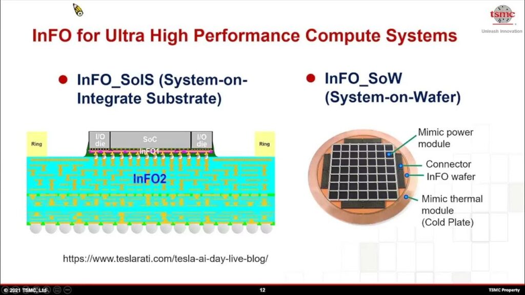
TSMC’s approach leverages existing technologies:
InFO-SoW: This integrates multiple chips onto a single interposer layer, offering advantages like shorter interconnects and improved performance.
System on Integrated Chips (SoIC): This stacks logic chips (processors) directly on top of memory chips (like HBM), creating a tighter integration.
Benefits:
- SoW promises significant advantages for AI applications in data centers.
- By integrating multiple chips on a single wafer, it can lead to:
- Increased compute power
- Reduced data center footprint
- Boosted performance per watt (energy efficiency)
- Current Status: The first iteration, a logic-only wafer based on InFO technology, is already in production.
2. Chip-on-Wafer (CoW-SoW) on the horizon:
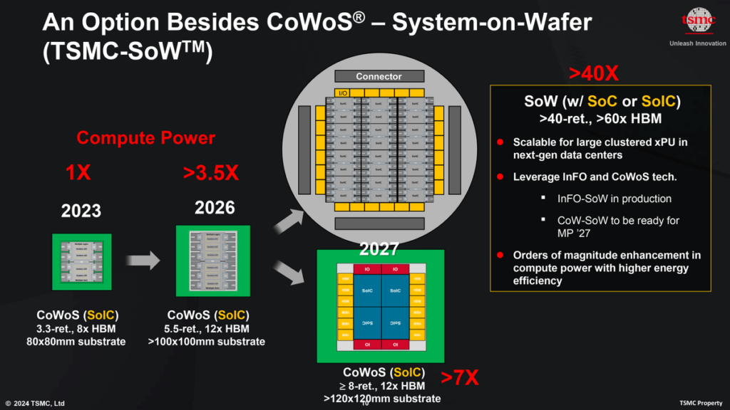
The next step, Chip-on-Wafer (CoW-SoW), is expected for mass production in 2027 . This will allow stacking memory or logic on top of a system-on-wafer using their Chip-on-Wafer (CoW) method . The initial target seems to be integrating HBM4 memory with wafer-scale processors.
This is the next stage of TSMC’s SoW roadmap, expected for volume production in 2027.
It builds upon the foundation of SoW by introducing a “layering” concept:
- A “base chip” forms the foundation of the wafer.
- Additional chips, like memory or logic, are then stacked on top using CoW technology.
Benefits: CoW-SoW offers even greater integration possibilities compared to the initial SoW design.
- It allows for a wider variety of chip combinations, potentially leading to even more powerful and efficient data center systems.
- The initial target seems to be integrating high-bandwidth memory (HBM4) with wafer-scale processors.
Tesla’s Dojo Training Tile:
A notable application of TSMC’s current wafer-scale technology is evident in Tesla’s Dojo training tile.
This innovative accelerator leverages wafer-scale integration to deliver high-performance computing for artificial intelligence applications.
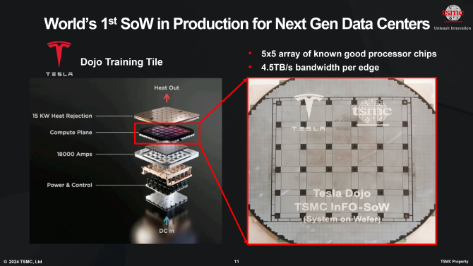
By utilizing pretested logic dies and advanced interconnect technology, Tesla’s Dojo exemplifies the potential of wafer-scale computing in driving AI innovation.
The Roadmap to 2027:
Looking ahead, TSMC has outlined an ambitious roadmap for wafer-scale computing, set to culminate in significant advancements by 2027.
The company plans to introduce more complex wafer-scale systems capable of delivering 40 times the computing power of current systems.
These advancements will leverage TSMC’s advanced packaging technologies, such as chip-on-wafer-on-substrate (CoWoS) and system-on-integrated chips (SoIC).
Read More: What are Emerging Memories: Types and Advantages
Implications for the Semiconductor Industry:
TSMC’s wave of wafer-scale computing technology carries profound implications for the semiconductor industry.
By enabling the integration of multiple dies on a single wafer, this approach promises to increase computing power while reducing energy consumption and footprint.
Moreover, it opens new possibilities for a wide range of applications beyond AI, including data centers, networking, and more.
Read More:AI GPU Market 2024: NVIDIA dominates with $40B, AMD rises to $3.5B, Intel lags at $500M – techovedas
Collaborations and Innovations:
Key to TSMC’s success in wafer-scale computing is its collaboration with industry partners and ongoing innovations in packaging technology.
Collaborations with companies like Cerebras and Nvidia have paved the way for pioneering applications of wafer-scale integration.
Additionally, ongoing research and development efforts continue to push the boundaries of what’s possible with wafer-scale computing.
Read More:4 Ways TSMC is Scaling Below 2nm and Beyond – techovedas
Future Applications and Opportunities:
Beyond AI training, wafer-scale computing holds immense potential for a variety of applications and industries.
From data centers to network infrastructure, the scalability and performance offered by wafer-scale technology can revolutionize how we process and analyze data.
Moreover, emerging technologies like Silicon-Interconnect Fabric (Si-IF) present new opportunities for integrating power management and other features into wafer-scale systems.
Conclusion:
As TSMC continues to advance its wafer-scale computing technology, the future of computing looks increasingly promising.
From the current iteration powering AI accelerators to the anticipated advancements by 2027, wafer-scale integration is poised to reshape the landscape of technology.
With its potential to drive innovation and unlock new possibilities, TSMC’s wave of wafer-scale computing heralds a new era in computing.