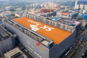
Introduction:
In a world increasingly reliant on semiconductor technology, the demand for skilled semiconductor engineers is soaring. However, meeting this demand poses significant challenges, especially in regions like India where establishing a robust semiconductor industry requires a skilled workforce. Lam Research Corp., a global leader in semiconductor equipment and services, has taken a pioneering step towards addressing this challenge through its Semiverse Solutions initiative.
Follow us on Linkedin for everything around Semiconductors & AI
Collaborative Memorandum of Understanding (MoU):
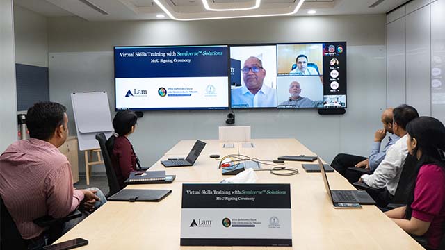
Lam Research recently announced the signing of a tripartite memorandum of understanding (MoU) with the India Semiconductor Mission (ISM) and the prestigious Indian Institute of Science (IISc).
Over the course of the next two years, Lam Research will be contributing software licenses valued at almost $29 million (equivalent to approximately INR 241 crores) to facilitate the education of 2800 students. Concurrently, the India Semiconductor Mission (ISM) will be backing the setup of necessary infrastructure and operational expenses. Furthermore, the Indian Institute of Science (IISc) will be taking on the responsibility of training instructors at designated universities. Lam Research will mobilize a specialized team of employees to assist in the nationwide expansion efforts.
This collaboration aims to revolutionize semiconductor workforce development in India through the deployment of Semiverse Solutions. Semiverse is Lam’s innovative virtual learning and collaboration platform.
Pilot Program Success and Expansion:
The journey towards this collaboration began with a pilot program announced as part of a joint statement issued by the governments of the United States and India in June 2023. The successful completion of the pilot program with IISc paved the way for the expansion of Semiverse Solutions to multiple universities across India.
This expansion is supported by Lam’s commitment of nearly $29 million in software licenses over the next two years, enabling 2800 students to access the platform.
Read More: Semiconductor Equipment Engineering: A Quiz Journey
Innovative Virtual Learning Environment:
At its core, Semiverse Solutions leverage Lam’s extensive portfolio of virtual technology. This includes processing, and simulations to create a boundary-less virtual learning environment. This platform not only fosters creativity and drives innovation but also significantly reduces costs and carbon footprint associated with traditional semiconductor training methods.
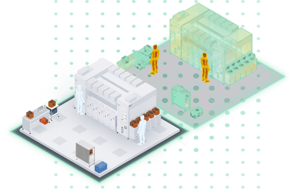
Lam Research uses the Semiverse to create a:
- Virtual representation: Think digital twins of real-world semiconductor fabrication processes.
- Collaborative environment: This virtual space allows researchers, designers, and manufacturers to work together seamlessly across geographical boundaries.
- Platform for innovation: By simulating and modeling processes virtually, Semiverse aims to accelerate chip development and problem-solving.
So, Semiverse is essentially a virtual world designed to improve collaboration and innovation within the semiconductor industry.
Read More: 9 Job Profiles For Diploma Holders in a Semiconductor Fab
Collaborative Roles:
The collaboration between Lam, ISM, and IISc is multifaceted. ISM supports the establishment of infrastructure and operational costs, while IISc plays a crucial role in training-the-trainers at selected universities. Lam, on the other hand, deploys a dedicated team of employees to support the expansion of Semiverse Solutions across the country.
“It’s exciting to embark on this journey with Lam Research and the IISc. As the semiconductor ecosystem in India grows, effective skill development partnerships will be key to ensuring we can sustain the momentum,”
~Akash Tripathi, CEO, ISM.
Impact and Future Goals:
The impact of Semiverse Solutions is already evident, with the pilot program training 35 engineers over a six-month period. Impressively, two participants from the pilot have been placed in global tier-1 semiconductor manufacturing companies. This underscores the effectiveness of the initiative.
“With two of the pilot’s participants already placed in a global tier-1 semiconductor manufacturing company, we are confident about the broad rollout of the course and its impact,”
~Professor Srinivasan Raghavan, Chair of the Centre for Nano Science and Engineering at IISc.
Looking ahead, the Semiverse Solutions initiative aims to educate up to 60,000 Indian engineers in semiconductor fabrication technologies over a ten-year period.
Read More: Job Alert! TATA Electronics Announces its First Hiring Drive for Dholera Plant in Gujarat
Global Significance:
The significance of this initiative extends beyond India’s borders. The semiconductor industry globally faces a talent shortage, making effective skill development partnerships imperative. By democratizing engineering skills training and improving access to talent pools through virtual labs, Semiverse Solutions offers a sustainable solution to this pressing challenge.
Conclusion:
In conclusion, Lam Research’s Semiverse Solutions initiative represents a bold step towards bridging the semiconductor talent gap in India and beyond.