Introduction
TechInsights recently made an unexpected technological leap by uncovering a groundbreaking 232-layer Quad-Level Cell (QLC) 3D NAND memory chip within a consumer device, marking World’s most advanced memory achievement from China
This discovery has far-reaching implications for the realm of high-performance computing (HPC), particularly in applications such as artificial intelligence (AI) and machine learning.
China’s Yangtze Memory Technologies Co., Ltd. (YMTC) has created a chip that represents a significant stride forward in memory chip design and is poised to reshape the landscape of advanced memory technology.
In this blog post, we will delve into the key takeaways from this discovery, providing in-depth insights into this groundbreaking development and its potential impact on the tech industry.

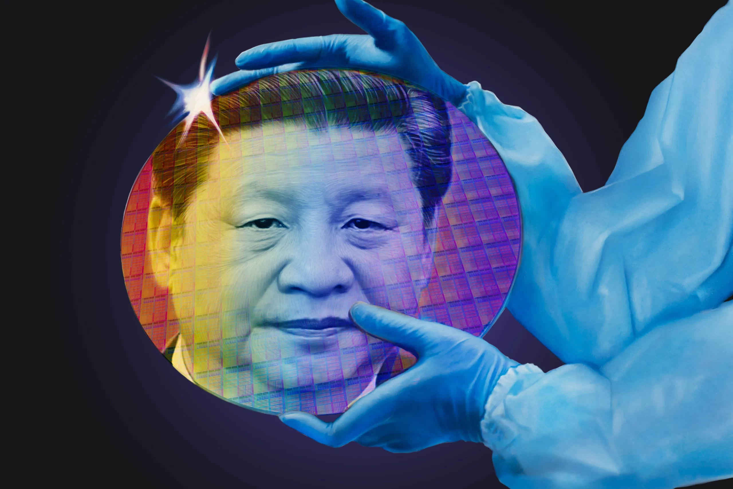
Image Credit: TechInsights
The Most advanced Memory from China
The star of this discovery is the remarkable 232-layer QLC 3D NAND die developed by YMTC, as illustrated above.
This cutting-edge chip is the core component of the ZhiTai Ti600 1TB solid-state drive (SSD), and it boasts an astonishing bit density of 19.8 Gb/mm², a milestone never before achieved in a commercially available NAND product.
Read More: How China Circumvented US Restrictions to Unveil 120 Layer NAND Flash
What is 232-Layer QLC 3D NAND ?
A 232-layer 3D NAND is advanced computer memory. Think of it as a skyscraper with tiny storage units as floors. Unlike flat two-dimensional memory chips, 3D NAND stacks these units, much like skyscraper floors.
So, a 232-layer 3D NAND has 232 layers of these storage units stacked on top of each other.
Each of these layers can store data, like your photos, videos, and documents. Having 232 layers means there’s a lot of space to store a huge amount of data.
This technology is vital for high-performance tasks like AI and fast data storage. It’s akin to a tall bookshelf with many shelves, each holding lots of books or data.
The more layers you have, the more books (or data) you can store in the same amount of space.
A 232-layer 3D NAND is significant as it offers faster and roomier digital storage. The controversy over this tech, amidst a U.S. ban, extends beyond its development. It involves national security, economic competition, and trade policies, adding to the concerns.
Read More: 1 TB chip: SK Hynix’s 321 layer Flash Revolution

Image Credit: TechInsights
Key Takeaways from Most Advanced Memory from China
Xtacking Hybrid Bonding Technology:
YMTC showcased the effectiveness of Xtacking Hybrid Bonding tech for 3D NAND TLC and QLC. BSSC technology in Xtacking 3.0 232L improved yield, performance, and cut production costs.
This highlights YMTC’s mastery of advanced memory chip technology.
Overcoming Sanctions:
Despite sanctions affecting Apple supplies and being on the U.S. entity list, YMTC perseveres in memory tech. The discovery showcases China’s resolve to overcome trade barriers and create a domestic semiconductor supply chain, demonstrating boundless innovation.
Competitive Edge:
In a memory industry downturn, YMTC’s cost-effective approach has given them an edge. Their high-bit-density 3D Xtacking NAND surpasses Micron and Intel, who are also working on 232-layer QLC 3D NAND.
Read More: Why is Foxconn, a Taiwan-based iPhone-maker being investigated by China

Image Credit: TechInsights
Competitors:
This discovery places YMTC ahead of companies like Micron and Intel (Solidigm) in the development of 232-layer QLC 3D NAND devices.
It’s important to note that Samsung has chosen not to develop QLC technology on its 236-layer (V8) 3D NAND chips, as their current strategy centers on advancing the V9 3D NAND TLC and QLC.
However, during Samsung’s recent Memory Tech Day, they introduced their first QLC product aimed at the mobile market, a 512GB UFS 3.1 product utilizing 176-layer (V7) technology.
Meanwhile, SK Hynix primarily focuses on TLC (Triple-Level Cell) devices rather than QLC (Quad-Level Cell) products.
| Company | Type of Memory | Development Status of 232-Layer NAND | Additional Notes |
|---|---|---|---|
| YMTC (China) | QLC (Quad-Level Cell) | Leading in 232-Layer QLC NAND development | – YMTC is ahead in the 232-layer QLC NAND race. |
| Micron (USA) | QLC (Quad-Level Cell) | Actively working on 232-Layer QLC NAND | – Competing in the development of 232-layer QLC NAND. |
| Intel (Solidigm) (USA) | QLC (Quad-Level Cell) | Working on 232-Layer QLC NAND | – Intel’s subsidiary Solidigm is in the race for 232-layer QLC NAND. |
| Samsung (South Korea) | V9 3D NAND TLC and QLC (Triple-Level Cell and Quad-Level Cell) | Focusing on V9 3D NAND TLC and QLC | – Samsung is concentrating on V9 3D NAND TLC and QLC technology. |
| Samsung (South Korea) | V7 3D NAND QLC (Triple-Level Cell) | Recently introduced 176-layer (V7) QLC NAND for mobile products | – Samsung has now ventured into QLC technology for mobile devices. |
| SK Hynix (South Korea) | TLC (Triple-Level Cell) | Focused on TLC (Triple-Level Cell) devices | – SK Hynix emphasizes TLC NAND rather than QLC NAND. |
What are the various memory innovations in the world?
Types of Memory:
QLC (Quad-Level Cell):
- Simple Explanation: QLC is a type of memory that can store a lot of data in each storage unit (cell). It’s like having four different levels of information that can be stored in one place.
- Usage: QLC memory is good for large storage devices like hard drives and SSDs where you need a lot of space to store photos, videos, and other big files.
TLC (Triple-Level Cell):
- Simple Explanation: TLC memory stores three levels of information in each storage unit. It’s a balance between speed and storage space.
- Usage: TLC is often used in consumer-grade SSDs because it provides a good mix of storage capacity and performance.
V9 3D NAND TLC (Triple-Level Cell) and QLC (Quad-Level Cell):
- Simple Explanation: V9 3D NAND memory is a type of memory that stacks data in three dimensions (similar to a skyscraper) and has the capacity to accommodate three or four levels of data in each cell.
- Usage: High-performance applications like top-tier SSDs for gaming and professional work use V9 3D NAND memory.
Comparison:
| Type of Memory | Explanation | Common Usage |
|---|---|---|
| QLC (Quad-Level Cell) | Stores four levels of data in each cell, providing a lot of storage space but may be slower. | Large storage devices like hard drives and budget-friendly SSDs. |
| TLC (Triple-Level Cell) | Stores three levels of data in each cell, offering a balance between storage space and speed. | Consumer-grade SSDs for everyday use. |
| V9 3D NAND TLC (Triple-Level Cell) and QLC (Quad-Level Cell) | Stacked memory with three or four levels of data in each cell, suitable for high-performance applications. | Top-tier SSDs for gaming, professional work, and advanced computing. |
Implications for the Industry from most advanced memory from China
YMTC’s groundbreaking achievement not only highlights the growing influence of Chinese semiconductor manufacturers but also underscores the broader trend of technological innovation in the face of trade restrictions.
China’s relentless pursuit of self-reliance in the semiconductor industry is yielding more successful results than initially anticipated, posing a significant challenge to established industry leaders.
This breakthrough in 3D NAND memory technology carries vast implications for high-performance computing applications, particularly in the domains of AI and machine learning.
It signifies a significant leap forward in memory technology and underscores the importance of fostering innovation, even when faced with complex geopolitical and economic hurdles.
Read More: China Restricts Exports of Graphite, in response to US Ban
Conclusion
YMTC’s 232-layer QLC 3D NAND discovery showcases China’s rise in the global semiconductor industry. Chinese tech firms, despite obstacles, are pushing the boundaries of chip design and production. This strengthens China’s tech position and highlights innovation’s crucial role in progress. As China’s semiconductor capabilities evolve, the tech industry is set for more advances.