Introduction
As artificial intelligence (AI) continues to evolve and integrate deeper into various industries, the demand for more efficient, powerful, and scalable hardware is becoming increasingly critical. Key innovations in semiconductor technology are playing a pivotal role in meeting these demands. Among these advancements, Gate-All-Around (GAA) transistors, 3D NAND memory, and High Bandwidth Memory (HBM) stand out as crucial enablers of AI’s future. This blog post delves into how these technologies are shaping the next generation of AI capabilities.
1. Gate-All-Around (GAA) Transistors: A New Era of Efficiency and Performance
What are GAA Transistors?
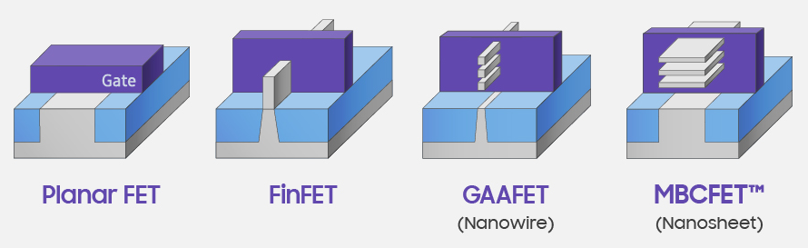
GAAFET stands for Gate-All-Around Field-Effect Transistor. Imagine a conventional FET (Field-Effect Transistor) as a water faucet. The gate acts like the handle, controlling the flow of water (current) through a channel. In a traditional FET, the gate only controls the flow from one or two sides.
A GAAFET is like a more advanced faucet design. Here, the gate completely surrounds the channel, like a ring around a hose. This allows for much finer control over the water flow.
Here’s how they differ:
Gate Control: Conventional FETs have limited control as the gate doesn’t fully surround the channel. GAAFETs, with their all-around gate, have superior control, leading to better performance.
Miniaturization: As we make transistors smaller, leakage (unwanted water flow) becomes a problem. The full gate control in GAAFETs helps minimize leakage even at tiny sizes. Conventional FETs struggle with this at very small scales.
Performance: Because of the tighter control and reduced leakage, GAAFETs can be faster and more efficient than conventional FETs.
Think of GAAFETs as the next generation of faucets. They offer superior control and performance for precise water management.
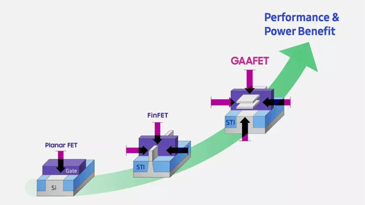
Consequently, the semiconductor industry is turning to Gate-All-Around (GAA) transistors to overcome these limitations. GAA transistors offer improved electrostatic control, reduced leakage currents, and enhanced performance compared to FinFETs.
GAA transistors, however, offer a novel approach where the gate material surrounds the channel region on all sides. This structure provides better control over the channel, reducing leakage current and improving overall performance.
Read More: 8 Companies Poised to Benefit Significantly from the AI Boom
Benefits for AI
Enhanced Performance: The superior electrostatic control of GAA transistors translates to higher performance and faster switching speeds, crucial for the heavy computational demands of AI algorithms.
Reduced Power Consumption: Improved control over leakage currents results in lower power consumption, which is vital for energy-efficient AI systems, especially in data centers and mobile applications.
Scalability: As semiconductor nodes shrink, GAA transistors are more scalable than FinFETs, supporting the continued miniaturization of components and enabling more powerful AI processors.
Read More: 5 Most Exciting Startups Building AI Hardware – techovedas
2. 3D NAND Memory: Elevating Data Storage Capabilities
What is 3D NAND Memory?
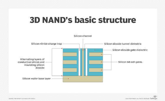
Imagine a traditional apartment building with a single floor. Each apartment represents a storage unit in the memory.
Conventional NAND: This is like building more and more apartment buildings with a single floor (more chips) to increase storage space. It works, but you’re limited by the available space.
3D NAND: This is like building the same number of buildings but adding more floors to each one (stacking memory cells vertically). It allows you to store much more information in the same footprint.
3D NAND memory is an advanced type of flash memory where memory cells are stacked vertically in multiple layers. Unlike traditional planar NAND, which is limited by the two-dimensional plane, 3D NAND, therefore, overcomes density limitations by extending into the third dimension.
Here’s how 3D NAND differs from conventional NAND:
Density: 3D NAND packs more storage capacity into a smaller space by stacking memory cells vertically.
Performance: While not as fast as the main memory (DRAM) in your computer, 3D NAND offers faster read and write speeds compared to traditional NAND.
Cost: Initially, 3D NAND was more expensive to manufacture. However, as the technology matures, the cost becomes more comparable to traditional NAND.
So, 3D NAND is like a clever way to maximize storage space in a city with limited land, while conventional NAND keeps expanding outwards.
Benefits for AI
Higher Storage Density: By stacking memory cells, 3D NAND significantly increases storage density, allowing for greater data storage capacity within the same footprint. This is essential for AI applications that require vast amounts of data.
Improved Reliability and Longevity: 3D NAND’s architecture reduces the wear on individual cells, enhancing the reliability and lifespan of memory, which is critical for continuous AI operations.
Faster Data Access: Innovations in 3D NAND technology also bring about faster read and write speeds, enabling quicker data retrieval and processing, thus accelerating AI model training and inference.
Read More: 6 Reasons Why Nvidia Overtook Apple as World’s Second Most Valuable Company – techovedas
3. High Bandwidth Memory (HBM): Revolutionizing Data Transfer
What is High Bandwidth Memory?
HBM stands for High-Bandwidth Memory. It’s a special type of memory designed for high-performance needs. Imagine you have a library for your computer’s data. Here’s how HBM differs from conventional memory (like DDR):
Conventional Memory (DDR): This is like a traditional library with bookshelves lining the walls. Librarians (memory controllers) have to walk up and down aisles (data bus) to find and retrieve information (data) from specific books (memory cells).
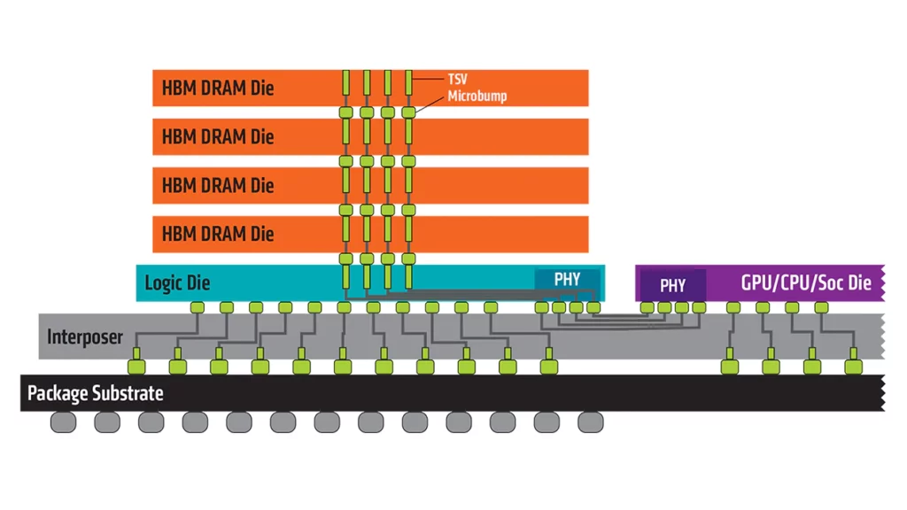
HBM (High-Bandwidth Memory): This is like a modern library with multiple floors and a central information desk. Librarians can quickly access information through a network of elevators (high-bandwidth channels) directly connecting them to the specific floor (memory layer) where the book (data) is stored.
Moreover,HBM achieves this by stacking multiple DRAM dies vertically and interconnecting them with through-silicon vias (TSVs), resulting in a compact, high-speed memory solution.
Here’s what makes HBM special:
- Speed: HBM boasts a much wider data highway compared to conventional memory. This allows for significantly faster transfer of information between the processor and memory.
- Size: HBM stacks multiple memory layers vertically, saving space compared to traditional memory modules with several memory chips laid out flat.
- Power Efficiency: The shorter distances within the stacked memory layers in HBM lead to lower power consumption for data transfer.
HBM is a high-tech library designed for super fast information retrieval. It’s perfect for applications handling massive amounts of data, like AI and high-end graphics processing.
Benefits for AI
Exceptional Speed: HBM provides high data transfer rates, which is essential for AI workloads that require rapid movement of large datasets between memory and processing units.
Energy Efficiency: Despite its high performance, HBM is more energy-efficient compared to traditional DRAM, reducing the overall power consumption of AI systems.
Compact Form Factor: The 3D stacking of HBM reduces the physical space required for memory, allowing for more compact and integrated AI hardware solutions.
The Synergy of GAA, 3D NAND, and HBM in AI
The convergence of GAA transistors, 3D NAND memory, and HBM creates a powerful trifecta that addresses the core challenges of AI hardware: performance, efficiency, and scalability.
- Performance Boost: GAA transistors and HBM work together to provide faster computation and data transfer speeds, enabling AI models to process information more rapidly.
- Enhanced Efficiency: Both GAA transistors and HBM contribute to lower power consumption, which is crucial for sustainable AI deployments, particularly in data centers where energy costs are a significant concern.
- Scalability and Density: The combination of 3D NAND’s high storage density and GAA transistors’ scalability supports the growing data needs of AI, while HBM’s compactness allows for more powerful and space-efficient designs.
Read More:6 Prerequisites for Pursuing M.Tech in VLSI: An In-Depth Guide – techovedas