Introduction:
In the intricate world of semiconductor manufacturing, precision is not just desirable; it’s absolutely essential. As chip designs become increasingly complex and feature sizes shrink to nanometer scales, traditional methods of lithography struggle to keep pace. Enter computational lithography, a revolutionary approach that combines the power of advanced algorithms and simulations to optimize the chip design process.
In this blog post, we’ll explore what computational lithography is, how it works, and why it’s transforming the landscape of chip design.
Follow us on LinkedIn for everything around Semiconductors & AI
Understanding Computational Lithography in Chip Design:
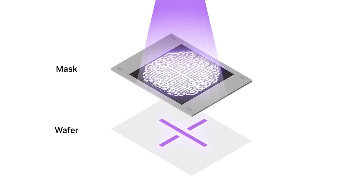
It is a computational approach to lithography, which is the process of transferring a pattern onto a substrate, typically a silicon wafer, during semiconductor manufacturing.
Moreover, in chip design,it utilizes sophisticated algorithms and simulations to optimize the entire lithographic process, from designing the mask layout to printing the patterns on the wafer.
Read More: How Nanoimprint Lithography Can Revolutionize Manufacturing – techovedas
Key Components of Computational Lithography:
Mask Optimization: Computational lithography optimizes the design of the mask, which contains the pattern that will be transferred onto the silicon wafer. By analyzing the characteristics of the mask, such as its shape, size, and pattern density, the software can generate a mask layout that maximizes the resolution and fidelity of the printed patterns.
Resolution Enhancement Techniques (RET): It employs a variety of resolution enhancement techniques to improve the printing resolution and pattern fidelity on the wafer.Moreover, these techniques may include optical proximity correction (OPC), phase-shifting masks, and source optimization, among others.
Process Window Optimization: One of the key advantages of computational lithography is its ability to optimize the lithographic process window, which refers to the range of process conditions (e.g., exposure dose, focus, and depth of focus) over which the desired patterns can be printed accurately. By simulating different process conditions, the software can identify the optimal settings that maximize yield and minimize defects.
Model-Based Simulations: It relies on rigorous mathematical models and simulations to predict the behavior of light as it interacts with the mask and the wafer. These models take into account various physial phenomena, such as diffraction, interference, and scattering, to accurately simulate the lithographic process and optimize the design parameters accordingly.
Read More: 5 Things to Know about High NA EUV Lithography; Revolutionizing Chip Manufacturing – techovedas
Let’s contrast computational lithography with conventional lithography in the context of chip design:
Design Complexity and Flexibility:
- Conventional lithography: In traditional lithography, designers are limited by the capabilities of the optical system and the mask. Moreover, Complex designs may require multiple exposures or compromise on resolution.
- Computational lithography:It offers greater design flexibility by utilizing advanced algorithms and simulations.Moreover, It can handle complex designs more efficiently and optimize them for better resolution and manufacturability.
Resolution Enhancement:
- Conventional lithography: Resolution enhancement techniques (RET) such as optical proximity correction (OPC) and phase-shifting masks are used to improve resolution. However, they have limitations in pushing the resolution to the desired levels for advanced nodes.
- Computational lithography:It mploys model-based simulations and sophisticated algorithms to enhance resolution further. It can predict and compensate for various physical effects, allowing for finer feature sizes and improved pattern fidelity.
Process Window Optimization:
- Conventional lithography: Traditional methods rely on empirical tuning of process parameters to achieve optimal results within the process window. Moreover, this can be time-consuming and may lead to suboptimal outcomes.
- Computational lithography: It optimizes the lithographic process window through rigorous simulations. By systematically analyzing process conditions, it identifies the optimal settings that maximize yield and minimize defects, leading to improved manufacturing efficiency.\
Cost and Time Efficiency:
- Conventional lithography: Traditional lithography techniques may require extensive trial-and-error iterations to achieve satisfactory results, leading to increased costs and longer development cycles.
- Computational lithography: By leveraging advanced algorithms and simulations, computational lithography reduces the need for physical experimentation and accelerates the design process. This results in cost savings and shorter time-to-market for semiconductor products.
Scalability:
- Conventional lithography: As feature sizes shrink to nanometer scales, conventional lithography faces challenges in maintaining resolution and pattern fidelity.
- Computational lithography: It offers a scalable solution to overcome the limitations of traditional lithography.Moreover,it can adapt to evolving technology nodes and continue to push the boundaries of semiconductor technology.
In summary, computational lithography offers significant advantages over conventional lithography in terms of design flexibility, resolution enhancement, process window optimization, cost efficiency, and scalability. By harnessing the power of advanced algorithms and simulations .It is revolutionizing chip design and driving innovation in the semiconductor industry.
Benefits of Computational Lithography in Chip Design:
- Improved Resolution: Computational lithography enables chip designers to achieve higher resolution and finer feature sizes than traditional methods, thereby pushing the boundaries of semiconductor technology.
- Enhanced Yield and Manufacturing Efficiency: By optimizing the lithographic process window and reducing defects, computational lithography improves yield and manufacturing efficiency, ultimately reducing costs and time-to-market for semiconductor products.
- Design Flexibility: Computational lithography provides chip designers with greater flexibility to explore complex design patterns and geometries, enabling them to create more innovative and advanced semiconductor devices.
- Cost-Effective Scaling: As semiconductor technology continues to scale down to smaller feature sizes, computational lithography offers a cost-effective solution to overcome the limitations of traditional lithography and extend Moore’s Law.
Read More: What are the Various Types of Semiconductor Packaging
Conclusion:
Computational lithography is revolutionizing the field of chip design by providing designers with powerful tools to optimize the lithographic process and push the boundaries of semiconductor technology.
By harnessing the power of advanced algorithms and simulations, it enables chip designers to achieve higher resolution, improved yield, and greater design flexibility than ever before.
As semiconductor technology continues to evolve, it will play an increasingly critical role in driving innovation and advancing the state-of-the-art in chip design


Thanks for sharing. I read many of your blog posts, cool, your blog is very good.