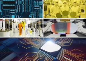
Introduction:
Chip packaging is not a one-size-fits-all solution; rather, it must be tailored to meet the specific requirements of different semiconductor applications. Whether it’s microprocessors powering our computers, memory chips storing data, sensors detecting environmental changes, or RF devices enabling wireless communication, each application demands unique packaging design variations.
In this detailed blog post, we’ll explore how packaging design considerations differ across various semiconductor applications, with real-world examples illustrating their importance.
Follow us on LinkedIn for everything around Semiconductors & AI
How Does Chip Packaging Change From Microprocessors to RF Devices
1. Microprocessors: Chip Packaging
Performance: Packaging for microprocessors must prioritize high-speed communication and low latency to ensure efficient data processing. Microprocessors generate a lot of heat due to high transistor density. Packages for these chips use materials like copper for heat sinks and thermal paste to transfer heat away from the die.
Advanced packaging techniques such as flip-chip BGA (Ball Grid Array) or 3D stacking improve signal integrity and thermal management. They help microprocessors achieve superior performance.
Signal integrity matters, but not as critical: Microprocessors operate at high speeds, but within the chip itself. The packaging needs to maintain good signal integrity within the package, but external connections are less critical for RF performance.
Examples
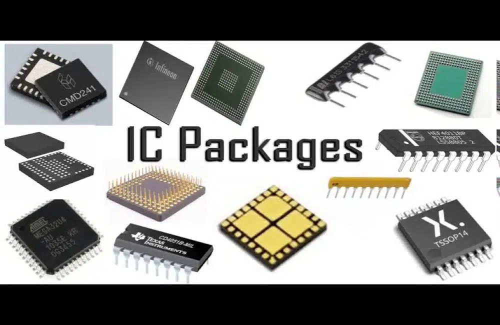
Quad Flat Package (QFP): A popular choice for microprocessors, QFPs have leads on all four sides for easy surface mounting on PCBs. They offer a good balance of heat dissipation and signal integrity.
Ball Grid Array (BGA): BGAs use solder balls on the underside of the package for connection. They offer higher pin count for complex processors and improved heat transfer due to the ball grid.
Read More: What are 5 Different Chip Packages: Advantages, Disadvantages & Applications – techovedas
2. Memory Chips: Chip Packaging
Density: Packaging for memory chips should maximize storage density while maintaining reliability and power efficiency. Focus on density and reliability: Memory chips prioritize storing as much data as possible in a small space. Manufacturers often use materials with high thermal conductivity to dissipate heat generated during operation while minimizing package size.
Signal integrity is important: While not as critical as RF devices, maintaining good signal integrity is crucial for accurate data read/write operations on memory chips.
Compact packaging solutions like chip-scale packages (CSPs) and wafer-level packaging (WLP) increase memory capacities in smaller sizes. They are perfect for mobile devices and data centers.
Examples
Small Outline Dual In-line Memory Module (SODIMM): Commonly found in laptops and small form-factor PCs, SODIMMs are small memory modules with pins on both sides for easy installation.
Ball Grid Array (BGA): Similar to microprocessors, BGAs are used for high-density memory chips like DDR4, offering compact size and good electrical performance.
Read More: $150 Million Power Play: South Korea Invests in the Future of Chip Packaging – techovedas
3. Sensors: Chip Packaging
Package needs to be compatible with sensor function: The packaging material can play a role in sensor performance. For example, pressure sensors might need a flexible package to allow pressure to reach the sensing element. Optical sensors might require a transparent window in the package.
Environmental protection: Many sensors need protection from the environment, such as moisture or harsh chemicals. The package material and sealing techniques are chosen accordingly.
Power efficiency can be a concern: Some sensors operate on low power, and the packaging should not introduce significant power losses.
Environmental Compatibility: Packaging for sensors must protect sensitive components from harsh environmental conditions while allowing for accurate data collection. Hermetic packages and conformal coatings shield sensors from moisture, dust, and temperature variations, ensuring reliable performance in diverse applications.
Examples:
Through-Hole Package (THP): THPs have pins that pass through holes in the PCB for secure mounting. They are often used for pressure sensors or other sensors requiring simple connections.
Land Grid Array (LGA): Similar to BGAs, LGAs use an array of solder lands for connection. They are used for sensors requiring a smaller footprint and higher pin count, like image sensors in cameras.
Bonding with specific materials: Certain sensors require specific packaging materials to function properly. For example, a pressure sensor might use a flexible membrane to transmit pressure to the sensing element.
4. RF Devices: Chip Packaging
To minimize signal loss, RF devices require packaging made of materials such as ceramics or high-performance plastics, as high-frequency signals are easily attenuated.
Signal Integrity: Packaging for RF devices must minimize signal loss and interference to ensure reliable wireless communication. RF-specific packaging techniques like RF CMOS system-in-package (SiP) integration enhance signal integrity and antenna performance. This optimization ensures robust connectivity in wireless devices.
Electromagnetic shielding is crucial: RF devices are sensitive to external electromagnetic interference (EMI) and can also generate EMI themselves. The package needs to be designed to shield the internal components and prevent EMI issues. This might involve metal cans or conductive layers within the package.
Matching impedance for optimal signal transfer: The package needs to be designed to match the impedance of the chip with the external circuit (usually 50 ohms). This ensures minimal signal reflection and efficient power transfer.pen_spark
Example:
Leadless Ceramic Package (LCP): These ceramic packages provide excellent electrical performance with minimal signal loss and good shielding. They are commonly used for high-frequency RF components like filters and amplifiers.
Cavity Package: Metal enclosures house the RF chip, offering superior shielding and controlled impedance for optimal signal transfer. They are used in applications like RF transceivers and power amplifiers.
Read More:AI GPU Market 2024: NVIDIA dominates with $40B, AMD rises to $3.5B, Intel lags at $500M – techo
Conclusion:
Packaging design considerations play a pivotal role in optimizing the performance, reliability, and functionality of semiconductor devices across diverse applications. By tailoring packaging solutions to meet the specific requirements of microprocessors, memory chips, sensors, and RF devices, semiconductor manufacturers can deliver products that excel in their respective fields.