Introduction:
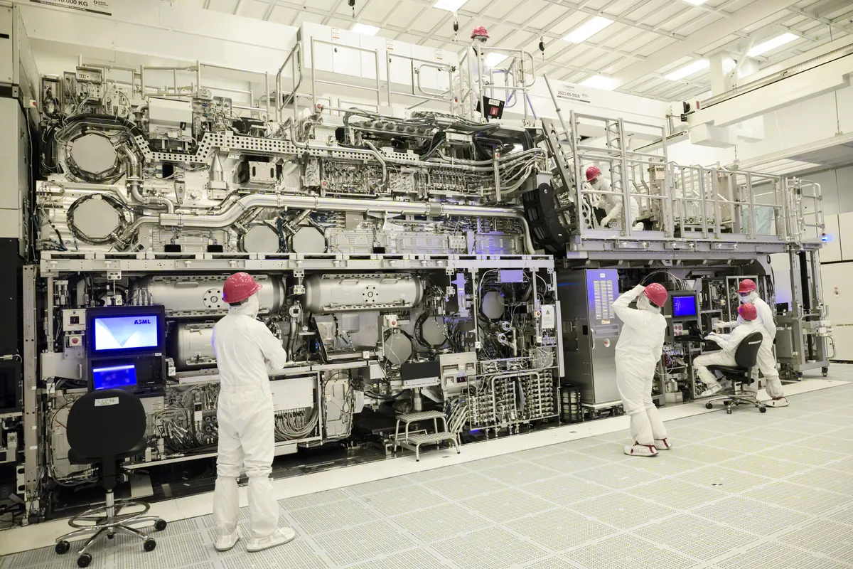
On Thursday, Intel Foundry achieved a significant milestone by completing the assembly of the industry’s inaugural commercial High Numerical Aperture (High-NA) Extreme Ultraviolet (EUV) machine at its D1X facility in Oregon. This development marks a crucial step as the company prepares for research and development on its 14A process set for 2025.
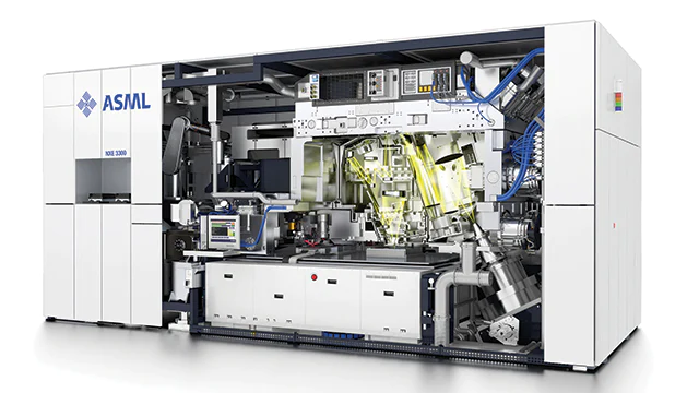
Intel is currently at the forefront of implementing High-NA EUV lithography, a significant advancement in chip manufacturing. Intel was the first company to acquire and assemble ASML’s High-NA EUV tool. High-NA EUV allows for smaller, faster chips with better performance and potentially lower power consumption. This is crucial for keeping up with the ever-growing demand for processing power.
Follow us on Linkedin for everything around Semiconductors & AI
Unveiling the High-NA EUV Journey: Intel’s Assembly Endeavor
As the lead customer for ASML’s Twinscan EXE:5000 machine, Intel Foundry has taken the lead in commencing R&D activities with this cutting-edge technology, surpassing competitors like TSMC.

The introduction of the High-NA lithography tool equips Intel with the capability to print features significantly smaller, up to 1.7 times, compared to existing EUV tools. This advancement positions Intel to produce smaller transistors than achievable with standard Low-NA EUV machines, potentially yielding up to a 2.9 times improvement in transistor density for a single exposure.
Notably, ASML announced yesterday that its other assembled High-NA machine, located in Veldhoven, Netherlands, achieved a noteworthy milestone by printing the first 10nm dense lines using a full-field lithography system, setting a new record for an EUV system.
The meticulous journey towards high-NA lithography has been meticulously documented by Intel, culminating in the recent completion of the first phase of assembly at its Oregon facilities.
Read More: What are Intel’s 10 largest Semiconductor Projects Worldwide – techovedas
History of Intel & (High NA)EUV:
Throughout its journey, Intel remained entrenched in the 14nm node, while its long-standing competitor TSMC embraced EUV technology and surged ahead in process node advancements, surpassing Intel for the first time. This allowed TSMC to equip Intel’s rivals, such as AMD, with superior process technology, leading to significant market share losses for Intel’s product division.
“With the addition of High NA EUV, Intel will have the most well-rounded lithography toolbox in the industry, enabling the company to drive future process capabilities beyond Intel 18A into the second half of this decade.”
–Mark Phillips, Intel Fellow and director of Lithography, Hardware and Solutions for Intel Foundry Logic Technology Development
Intel eventually adopted EUV technology with its ‘Intel 4’ process node, but extensive delays resulted in Intel lagging behind TSMC by several nodes. To regain its footing, Intel embarked on an ambitious initiative known as ‘5N4Y’ (Five Nodes in Four Years), which aims to launch five nodes within four years, with completion expected by the end of the year.

Despite these efforts, Intel recognizes that the journey toward technological leadership is ongoing and is committed to avoiding past mistakes by continuously embracing the latest technologies. Intel’s focus now shifts to the development of its newly unveiled ‘Intel 14A’ (1.4nm-class) process node and the subsequent 10A node (1nm), both leveraging High-NA EUV technology. Intel plans to mitigate risks by establishing product proof points with its 18A node in 2025 before progressing to the 14A node.
Additionally, Intel intends to be an early adopter of ASML’s second-generation Twinscan EXE:5200B system, boasting a throughput of over 200 wafers per hour (WPH), a notable improvement over the current-generation High-NA machine’s 185 WPH. These advancements position Intel ahead of ASML’s flagship Low-NA EUV machine, which offers a throughput of up to 160 WPH. Intel also notes that ASML is already developing three generations of its High-NA machines.
Read More: 3 Reasons Why TSMC Won’t Adopt High-NA EUV Lithography Until 2032
Conclusion: Shaping the Future of Semiconductor Fabrication
In conclusion, Intel’s foray into high-NA lithography represents a monumental leap forward in semiconductor fabrication. It is positioning the company at the forefront of technological advancement.