Introduction:
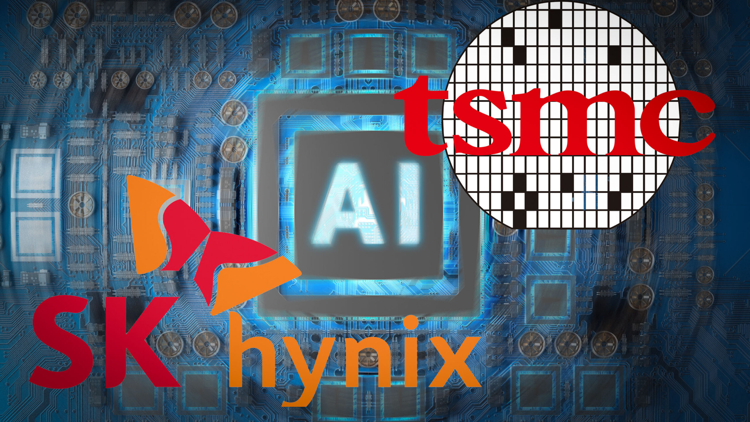
In an era where technological breakthroughs drive progress, the partnership between SK Hynix and TSMC marks a pivotal moment in memory innovation. Their joint venture aims to propel memory technology forward with the development of the sixth generation of High Bandwidth Memory (HBM4) by 2026.
This partnership leverages the strengths of both companies: SK Hynix’s expertise in memory and TSMC’s advanced chip manufacturing capabilities. The goal is to create a superior HBM solution that will benefit various industries, particularly those reliant on artificial intelligence and machine learning.
This blog post delves into the intricacies of this groundbreaking collaboration, exploring its technical aspects, economic ramifications, and potential implications for the semiconductor industry.
Follow us on Linkedin for everything around Semiconductors & AI
Partnership Announcement:
On April 19, 2024, SK Hynix and TSMC unveiled their strategic partnership to pioneer next-generation HBM4 memory and packaging technologies.
This collaboration represents a convergence of expertise between SK Hynix, a leading memory chip manufacturer, and TSMC, a renowned semiconductor foundry, both known for their contributions to the semiconductor landscape.
Read More: Atmanirbhar Bharat in Action: Kaynes to Build RUDRA Supercomputers – techovedas
Significance of HBM4:
HBM4 stands poised to revolutionize memory technology, promising unparalleled performance, energy efficiency, and scalability.
HBM4 stands for High Bandwidth Memory, version 4. It’s a new type of memory technology currently under development by SK Hynix and TSMC.
Here’s a breakdown of what we know so far:
High Bandwidth: As the name suggests, HBM4 is designed to offer significantly higher bandwidth compared to previous generations of HBM. This allows data to flow much faster between the memory and the processor.
Wider Interface: The biggest change expected in HBM4 is a wider memory interface. Currently, HBM uses a 1024-bit interface, but HBM4 might double that to 2048 bits [3]. This wider lane essentially allows for more data transfer simultaneously.
Performance Boost: The increased bandwidth of HBM4 translates to improved performance for applications that rely heavily on data movement, such as artificial intelligence, machine learning, and high-performance computing.
Collaboration Effort: Developing HBM4 requires expertise in both memory design and advanced chip manufacturing. That’s why SK Hynix, a memory specialist, and TSMC, a leading chip manufacturer, are working together on this project [5].
It’s important to note that HBM4 is still under development, and some details might change. However, the expected benefits for data-intensive applications are significant.
Read more 10 Fabrication Steps to Build a Semiconductor Chip – techovedas
Why does HBM Matter?
HBM4 is important for a few key reasons, particularly for applications that deal with massive amounts of data processing:
Faster AI and Machine Learning: HBM4’s increased bandwidth will be a game-changer for artificial intelligence (AI) and machine learning (ML). These fields rely heavily on processing large datasets, and HBM4’s ability to move data faster will significantly improve training times and overall performance. This can lead to faster development of AI models and quicker breakthroughs in various fields.
Enhanced High-Performance Computing (HPC): High-performance computing (HPC) applications also require significant data movement. HBM4 can significantly boost the speed and efficiency of these tasks, allowing researchers and scientists to tackle even more complex problems in fields like weather forecasting, climate modeling, and drug discovery.
Future-Proofing Technology: As data processing needs continue to grow, HBM4 provides a future-proof solution for demanding applications. Its higher bandwidth will be crucial for handling the ever-increasing data demands of emerging technologies like virtual reality (VR) and augmented reality (AR).
Efficiency Gains: Although not the primary focus, HBM4 is also expected to offer some improvements in power efficiency compared to previous generations. This can be beneficial for data centers that house large numbers of HPC and AI systems, as it can help reduce energy consumption costs.
Overall, HBM4 is a significant leap forward in memory technology. Its ability to handle massive data transfers at high speeds will be crucial for advancements in various fields that rely heavily on data processing.
Timeline and Goals:
The collaborative effort aims to achieve mass production of HBM4 by 2026, positioning both companies as frontrunners in memory innovation.
By leveraging TSMC’s state-of-the-art foundry process and SK Hynix’s expertise in memory design, the partners seek to expedite HBM4 development and push the boundaries of memory technology.
This ambitious timeline underscores their commitment to delivering groundbreaking solutions within a foreseeable timeframe.
Read More: Apple to Invest Over $250 Million in Expanding Singapore Campus – techovedas
Collaborative Efforts:
The collaboration extends beyond HBM4 development to encompass advancements in packaging technologies like CoWoS 2 (Chip-on-Wafer-on-Substrate).
Through synergistic efforts in product design, foundry processes, and memory integration, the partners aim to surpass performance limitations and unlock new frontiers in AI applications and GPU accelerators.
This holistic approach underscores the importance of interdisciplinary collaboration in driving innovation forward.
Read more 10 Fabrication Steps to Build a Semiconductor Chip – techovedas
Technical Focus:
A primary focus of the partnership is enhancing the performance and efficiency of the base die within HBM4 packages. By optimizing the integration of core DRAM dies and base dies with Through-Silicon Via (TSV) technology, the companies aim to maximize memory bandwidth, minimize latency, and optimize power consumption. Furthermore, research and development endeavors will explore novel materials, architectures, and manufacturing techniques to further enhance HBM4’s capabilities and reliability.
Read More: Jaishankar Encourages Singaporean Businesses to Invest in India’s Semiconductor Sector
Economic and Industry Implications:
The development of HBM4 has profound economic implications. It drives job creation and fosters innovation.
It bolsters the competitiveness of the semiconductor industry. SK Hynix and TSMC collaborating to bring HBM4 to market is expected to stimulate economic growth.
It will attract investment and reinforce their positions as leaders in the global memory market. Additionally, widespread adoption of HBM4 will catalyze demand for related technologies.
It will spur further advancements across the semiconductor ecosystem.
Read More:Top 10Trillion-Dollar Companies in 2024 – techovedas
Conclusion:
The partnership between SK Hynix and TSMC represents a transformative moment in memory technology, with HBM4 poised to redefine the semiconductor landscape.
By harnessing their combined expertise, resources, and vision for innovation, the two companies aim to accelerate the evolution of memory technology and address the evolving needs of emerging applications.
As the journey towards HBM4 unfolds, the industry eagerly anticipates the profound impact of this landmark collaboration, paving the way for a future defined by faster, more efficient, and more powerful memory solutions.