Introduction
In the ever-evolving landscape of semiconductor technology, breakthroughs are not just welcome but essential for progress. Recently, SK Hynix, one of the leading players in the memory chip industry, has been making waves with its testing of Tokyo E-Tech’s (TEL) latest -70°C etching tools. This move marks a significant step forward in the production of 3D NAND chips, promising more than 400 layers and potentially revolutionizing the industry.
Follow us on LinkedIn for everything around Semiconductors & AI
SK Hynix Quest for More Layers at -70°C
The demand for higher capacity and faster memory solutions is insatiable, driving companies like SK Hynix to explore innovative approaches. One such approach lies in stacking more layers within the same chip footprint, thereby increasing storage density without compromising performance. However, achieving this feat is no easy task.
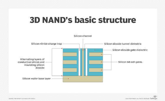
Traditionally, etching vertical holes in semiconductor structures has been a major challenge due to limitations in existing etching equipment. SK Hynix’s adoption of TEL’s new low-temperature etching tools opens up exciting possibilities by allowing for deeper memory channel holes with excellent uniformity.
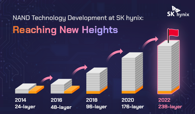
This breakthrough could pave the way for more than 400 layers of 3D NAND, a significant leap from current standards.
Read More:$42 Million: PSMC Opens New Factory to Produce 50,000 12-Inch Wafer including CoWoS – techovedas
The Power of -70°C Etching at SK hynix
TEL’s latest etching equipment operates at an ultra-low temperature of -70°C, a stark departure from conventional tools that work within the 0~30°C range. This enables faster and more precise etching processes, with the ability to complete 10-micron deep aspect ratio etching in just 33 minutes.
Operating at ultra-low temperatures can enhance etching processes in several ways:
Reduced Chemical Reaction Rates: Lower temperatures slow down chemical reactions, which can lead to more controlled and precise etching. This allows for finer detail and less deviation from desired patterns.
Reduced Etch Rate Variability: Temperature fluctuations can cause variations in etch rates, leading to inconsistencies in the final product. Operating at a consistently low temperature helps maintain stable etch rates, ensuring uniformity across the substrate.
Enhanced Selectivity: Lower temperatures can improve the selectivity of the etching process, meaning it can more precisely remove specific materials while leaving others intact. This is crucial for creating intricate semiconductor structures with high aspect ratios.
Improved Etch Depth Control: Etching at low temperatures can help control the depth of the etch more accurately, allowing for the creation of precise features with greater depth control. This is particularly important for applications such as 3D NAND manufacturing, where deep aspect ratio etching is required.
Such efficiency gains promise to reshape production timelines and enhance output quality, setting a new benchmark for 3D NAND manufacturing.
Moreover, the use of low-temperature etching offers environmental benefits by reducing carbon emissions. TEL’s equipment utilizes hydrogen fluoride instead of fluorocarbon, significantly curbing greenhouse gas emissions.
This aligns with broader industry efforts towards sustainability, with both SK Hynix and Samsung exploring ways to minimize their environmental footprint through technological innovation.
Reducing Costs, Increasing Efficiency
Beyond its technological implications, SK Hynix’s adoption of TEL’s etching tools holds significant economic potential. By stacking more layers using fewer stacks, memory manufacturers can streamline the manufacturing process, resulting in cost reductions.
The simplicity and efficiency afforded by this approach could lead to greater economies of scale, further driving down production costs and potentially lowering consumer prices for NAND-based products.
Looking Ahead
As SK Hynix continues its testing of TEL’s low-temperature etching tools, the industry eagerly anticipates the potential impact on 3D NAND production. With ambitions to surpass the 400-layer milestone, SK Hynix aims to push the boundaries of memory chip technology, setting new standards for capacity, performance, and efficiency.
Moreover, the environmental benefits of low-temperature etching underscore the industry’s commitment to sustainability, paving the way for greener semiconductor manufacturing practices.
Conclusion
In conclusion, the collaboration between SK Hynix and Tokyo E-Tech represents a significant advancement in semiconductor technology, with far-reaching implications for the memory chip industry. By harnessing the power of low-temperature etching, these companies are charting a course towards higher capacity, more efficient, and environmentally friendly memory solutions, shaping the future of digital storage.