Introduction
In the intricate landscape of semiconductor design, there exists a delicate balance between four crucial factors: Performance, Power, Area, and Cost (PPAC). For companies entrenched in the various stages of the semiconductor value chain—design, manufacturing, assembly, and integration—navigating this balance is paramount to the success of their products. In this article, we delve into the intricacies of PPAC and explore how design teams optimize semiconductor solutions to meet diverse application requirements.
Follow us on Linkedin for everything around Semiconductors & AI
Understanding PPAC Metrics
At the heart of semiconductor design lie the metrics of Performance, Power, and Area, each representing essential facets of chip functionality:
Performance: Often quantified in clock frequency (Hz), performance signifies the computational capability and speed of a semiconductor device. Higher performance is desirable for applications requiring rapid data processing and throughput.
Power: Measured in watts, power consumption denotes the energy efficiency of a chip. Lower power consumption is critical for battery-powered devices, where extending battery life is a primary concern.
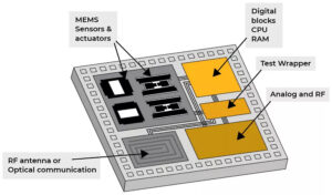
Area: Expressed in nanometers (nm), area refers to the physical size of the semiconductor chip. Smaller chip size enables higher integration density and reduced manufacturing costs.
Read More: China Bans Intel and AMD From Government Computers
The Trade-off Dilemma
In semiconductor design, achieving optimal PPAC balance necessitates trade-offs among these metrics. Design teams must make strategic decisions based on the specific requirements of the application:
Performance vs. Power: Consider a scenario where a chip is destined for a data center server. In this case, the primary focus may be on maximizing performance, leveraging ample space and a stable power source. However, for battery-powered devices like smartphones, minimizing power consumption takes precedence over raw performance.
Power vs. Area: In portable electronics such as wearables and IoT devices, minimizing power consumption is critical to prolong battery life. Consequently, design efforts often prioritize reducing chip area to accommodate smaller form factors and enhance portability.
Area vs. Performance: While some applications demand compact, energy-efficient chips, others prioritize raw computational power. High-performance computing (HPC) systems, for instance, prioritize performance over chip size, as space constraints are less significant in server environments.
Read more 80% Production Restored and No Impact on EUV: Earthquake Barely Bruises TSMC – techovedas
Optimization Strategies
To navigate these trade-offs effectively, semiconductor design teams employ various optimization strategies:
Architectural Innovation: Rethinking chip architecture and employing advanced design techniques can enhance performance without significantly increasing power consumption or chip area. Techniques such as pipelining, parallel processing, and hardware accelerators enable efficient use of resources.
Process Technology Advancements: Leveraging cutting-edge process technologies, such as FinFET and EUV lithography, enables semiconductor manufacturers to shrink chip sizes, reduce power consumption, and improve performance simultaneously.
Power Management Techniques: Incorporating dynamic voltage and frequency scaling (DVFS), power gating, and clock gating mechanisms allows for dynamic adjustment of power consumption based on workload demands, optimizing energy efficiency.
Design-for-Cost Methodologies: Employing design-for-cost principles early in the design phase helps mitigate manufacturing complexities and reduce production costs. Design teams focus on minimizing design iterations, optimizing yield, and streamlining manufacturing processes to meet cost targets.
Read More: HBM3e: AI’s Memory Marvel or Hype? Truth Behind SK hynix’s Game-Changer
Conclusion
In the realm of semiconductor design, the pursuit of PPAC optimization is a multifaceted endeavor. Design teams must strike a delicate balance between performance, power, area, and cost to meet the diverse needs of modern applications. By leveraging innovative design techniques, advanced process technologies, and cost-conscious methodologies, semiconductor companies can deliver high-performance, energy-efficient, and cost-effective solutions to the market.
In essence, the journey towards PPAC optimization embodies the relentless pursuit of technological advancement and the art of balancing competing priorities to push the boundaries of semiconductor innovation.