Introduction
In the ever-evolving landscape of mobile technology, where demands for faster speeds and increased bandwidth are incessantly on the rise, innovation becomes not just a buzzword but a necessity. Addressing this need head-on, United Microelectronics Corp (UMC) of Hsinchu, Taiwan, has recently made waves in the semiconductor industry with its groundbreaking announcement of the first-ever 3D IC solution for radio-frequency silicon-on-insulator (RFSOI) technology.
RFSOI technology is used in radio frequency (RF) applications, which are crucial for wireless communication devices like smartphones, IoT devices, and 5G infrastructure.
UMC is offering this 3D IC solution on their 55nm RFSOI platform. “55nm” refers to the size of the transistors and other components on the chip. The smaller the size, the more components can be packed onto the chip, leading to higher performance and efficiency.
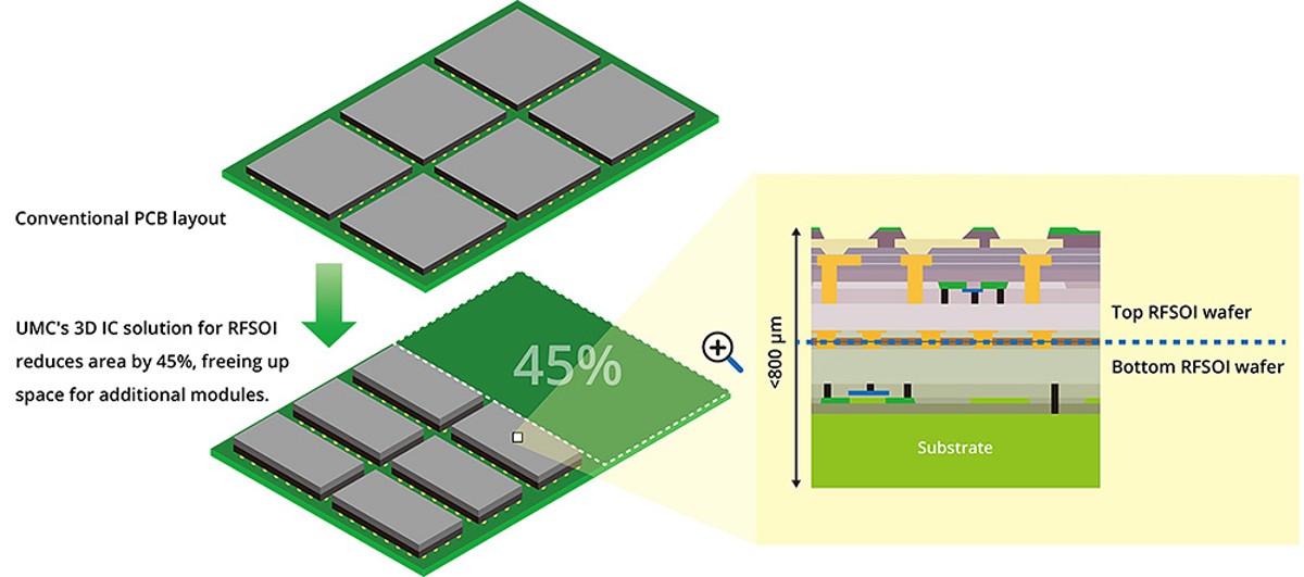
By implementing this new 3D IC solution, UMC claims to reduce the size of the chip by more than 45%. The reduction in size is significant because it enables the integration of more components onto the same chip, potentially enhancing functionality or performance.
Despite the reduction in size, UMC asserts that the RF performance of the chip remains unaffected. This is crucial for RF applications where performance and signal integrity are critical.
Follow us on LinkedIn for everything around Semiconductors & AI
“We are proud to lead the industry in offering this state-of-the-art solution utilizing our innovative 3D IC technology for RF-FEM. This groundbreaking technology not only solves the challenges of increased frequency band demands in smartphones in the 5G/6G era, but also helps in mobile, IoT, and virtual reality devices with faster data transfer by accommodating more frequency bands in parallel,” said Raj Verma, Associate Vice President of Technology Development at UMC. “We are excited to continue developing stacked die solutions to meet our customers’ RF needs, such as for 5G millimeter-wave, in the future.”
The term “3D IC solution for radio-frequency silicon-on-insulator (RFSOI) technology” encompasses several key concepts:

UMC 3D IC Solution:
This refers to a three-dimensional integrated circuit solution. Traditionally, integrated circuits (ICs) are fabricated in two dimensions, with all components positioned on a single plane. However, 3D integration involves stacking multiple layers of integrated circuits on top of each other, enabling enhanced functionality and density within a reduced footprint.
UMC RFSOI Technology:
RF SOI technology involves the fabrication of RF integrated circuits on a silicon substrate that is insulated (i.e., has an insulating layer such as silicon dioxide) from the underlying silicon substrate. SOI technology offers advantages for RF applications, such as improved isolation and reduced parasitic capacitance, which are crucial for high-frequency operation.
Read More: 4 Talks on Future of Semiconductor Industry by Intel Nvidia AMD and TSMC CEO – techovedas
UMC 3D Integration for RFSOI Applications:
The integration of RF components is particularly critical in modern electronic devices, especially in the context of wireless communication systems like smartphones and IoT devices. RF components include amplifiers, switches, filters, and antennas, which are essential for transmitting and receiving radio signals. Moreover, these components play a crucial role in various electronic devices, facilitating seamless communication and connectivity across different platforms.
Therefore, the phrase “3D IC solution for RFSOI technology” signifies a cutting-edge approach to integrating RF components using stacked ICs on a silicon-on-insulator substrate. This innovative solution offers benefits such as reduced size, improved performance, and enhanced integration capabilities, making it well-suited for addressing the increasing demands of wireless communication systems, including the transition to 5G and beyond.
Read More: 5 Step Method To Build Your First Electronic Gadget With Arduino – techovedas
Revolutionizing RFSOI Integration with UMC 3D
UMC has positioned its latest offering, based on its advanced 55nm RFSOI platform, to redefine how RF components integrate into mobile devices, especially amidst the growing 5G era.
With mobile device manufacturers facing the daunting task of accommodating an increasing number of frequency bands in smartphones, UMC’s 3D IC solution for RFSOI emerges as a game-changer.
By leveraging stacked silicon technology, UMC has achieved a remarkable reduction in die size, slashing it by over 45% without compromising on RF performance. This substantial reduction in surface area not only optimizes the utilization of space within devices but also paves the way for the seamless integration of additional RF front-end modules (RF-FEM). These modules play a pivotal role in transmitting and receiving data, thereby enhancing the overall functionality and performance of mobile devices.
Read More: 5 Step Method To Build Your First Electronic Gadget With Arduino – techovedas
Overcoming Interference Challenges
One of the key challenges inherent in vertically stacking dies is the potential for RF interference between layers. UMC, however, has effectively tackled this obstacle through the utilization of wafer-to-wafer bonding technology, ensuring the integrity and reliability of the stacked die configuration. This innovative approach not only mitigates RF interference but also lays the groundwork for enhanced signal integrity and performance.
Read More:Intel: A Story of Innovation – techovedas
Patented Excellence
UMC’s foray into 3D IC technology for RFSOI is underpinned by a robust portfolio of patents, attesting to the company’s commitment to pushing the boundaries of semiconductor innovation.
With multiple patents secured for its groundbreaking processes, UMC stands at the forefront of technological advancement. Moreover, poised to revolutionize RF integration in mobile devices and beyond, the company’s strides in this domain promise to reshape the landscape of semiconductor engineering.
Read More: $30 Billion: Meta’s Investment in NVIDIA GPUs to Supercharge AI Development – techovedas
A Vision for the Future
According to Raj Verma, Associate VP of Technology Development at UMC, the unveiling of this state-of-the-art 3D IC solution marks a pivotal moment in the industry’s trajectory. Beyond addressing the immediate challenges posed by the 5G/6G era, UMC’s innovative technology holds promise for a myriad of applications, including mobile, IoT, and virtual reality devices. As the demand for faster data transfer and greater bandwidth continues to escalate, UMC remains steadfast in its commitment to delivering tailored solutions that meet the evolving needs of its customers.
Read More: 3nm GAAFET: Samsung Tapes Out First Mobile SoC With Synopsys AI Tools – techovedas
Conclusion
In a landscape defined by relentless innovation and ever-expanding technological horizons, UMC’s pioneering 3D IC solution for RFSOI stands as a testament to the company’s unwavering dedication to excellence. By harnessing the power of stacked silicon technology and proprietary bonding processes, UMC has unlocked new possibilities in RF integration, ushering in a new era of connectivity and performance in mobile devices. As the industry continues to evolve, UMC remains poised to lead the charge, driving innovation and shaping the future of semiconductor technology.