Introduction:
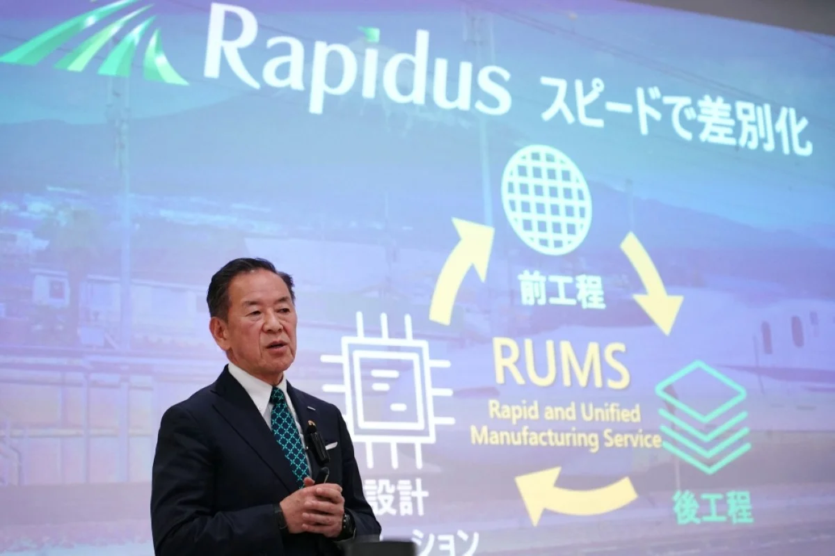
In a bid to bolster its semiconductor manufacturing capabilities and compete with industry giants like Taiwan Semiconductor Manufacturing Co (TSMC) and Samsung Electronics, Japan recently approved up to ¥590 billion (US$3.9 billion) in subsidies to chip venture Rapidus.
On Tuesday, Japan announced its approval of up to 590 billion yen ($3.89 billion) in additional subsidies for chipmaker Rapidus Corporation. The newly allocated support encompasses up to 53.5 billion yen designated for research and development in back-end processes like chip packaging, as outlined in a press briefing by Japan’s Ministry of Economy, Trade and Industry on Tuesday.
Between 2022 and 2023, Rapidus received 330 billion yen in funding from the Japanese government to facilitate the mass production of 2-nanometer chips in Chitose, Hokkaido, starting from 2027.
This significant investment underscores Japan’s strategic ambition to reclaim its position as a key player in the global semiconductor landscape.
Let’s delve into the details of this development and its implications for Japan’s semiconductor industry and the broader technological ecosystem.
Follow us on Linkedin for everything around Semiconductors & AI
Rapidus Chip Venture: Ambition and Collaboration
Rapidus is a newcomer in the semiconductor industry. It aims to mass-produce chips in Japan’s Hokkaido.
1nm Chips on the Horizon: Rapidus Aims to Produce 1 nm Node by 2027
Japan’s funding will speed up equipment acquisition and process advancement. Rapidus collaborates with IBM researchers to drive innovation.
Ambition:
- Become a leading chip manufacturer: Japan aims for Rapidus to compete with industry giants like TSMC. This requires developing cutting-edge chip production capabilities.
- Close the gap in chip technology: Japan currently lags behind in advanced chip manufacturing. Rapidus aspires to bridge this gap and make Japan a major player in the global chip market.
- Boost domestic chip production: The investment aims to reduce Japan’s reliance on foreign chip suppliers and strengthen its technological independence.
Collaboration:
- Partnership with IBM: This collaboration leverages IBM’s expertise in chip packaging technologies. Rapidus will benefit from IBM’s knowledge to improve chip performance and efficiency.
- Potential for further collaborations: The future might see Rapidus partnering with other research institutions or chip companies to access expertise and resources for chip development and manufacturing.
- Government support: The US$3.9 billion government aid signifies Japan’s commitment to collaborate with Rapidus to achieve its ambitious goals.
Overall, Rapidus’s ambition is to become a major force in the chip industry through collaboration with leading players and government support.
Read More:Innovation vs. Regulation: Can the US-UK AI Alliance Overcome the Divide? – techovedas
Government Support and Economic Significance:
The approval of US$3.9 billion in aid to Rapidus is part of Japan’s broader strategy to revitalize its semiconductor industry and enhance economic resilience.
Economy Minister Ken Saito emphasized the critical role of next-generation semiconductors in shaping Japan’s industry and economic growth trajectory.
With Japan committing billions of dollars into Rapidus’s venture, alongside other chip-making initiatives, the government aims to stimulate innovation, create high-value jobs, and strengthen the country’s technological capabilities.
Read More: How Did AI Influence Semiconductor Market Despite 2023’s Downturn? – techovedas
Global Implications and Geopolitical Dynamics:
The geopolitical landscape has witnessed a heightened focus on semiconductor manufacturing. This is driven by concerns over supply chain vulnerabilities and technological sovereignty.
Japan’s investment in Rapidus aligns with global trends, as governments worldwide prioritize domestic capabilities in semiconductor production.
Collaborations between Rapidus, IBM, and other industry players underscore a concerted effort to mitigate dependence on foreign suppliers and enhance national security in critical technology sectors.
Read More: 7.2 Magnitude Earthquake Hits Taiwan: TSMC and UMC Affected – techovedas
Challenges and Opportunities:
While Japan’s investment in Rapidus signals a significant step towards semiconductor self-sufficiency, challenges lie ahead.
Delays in licensing, subsidy allocations, and technology transfer processes pose hurdles to rapid progress.
However, Japan’s rich history of technological innovation, coupled with its commitment to semiconductor research and development (R&D), positions the country favorably to overcome these challenges and capitalize on emerging opportunities in the semiconductor market.
Read More: 5 International Tech Stocks Poised to Dominate the Next Decade – techovedas
Conclusion:
Japan’s approval of US$3.9 billion in aid to chip venture Rapidus marks a strategic move towards revitalizing its semiconductor industry and enhancing its global competitiveness.
With a focus on innovation, collaboration, and economic resilience, Japan aims to reclaim its position as a leading semiconductor manufacturer.


