Introduction:
Welcome to “A Brief History of the Field of VLSI” blog post, where we embark on a fascinating journey through the intricate world of Very Large Scale Integration (VLSI). VLSI technology represents a pivotal milestone in the evolution of modern electronics, enabling the integration of millions, if not billions, of transistors onto a single silicon chip. This remarkable advancement has revolutionized our lives, powering everything from smartphones and computers to medical devices and smart home appliances.
In this post, we’ll explore the origins, key developments, and transformative impacts of VLSI. We’ll glimpse the incredible progression of this critical technology. Join us to unravel how VLSI has reshaped electronics and paved the digital age we live in.
Follow us on Linkedin for everything around Semiconductors & AI
1. Invention of Transistor (1947)
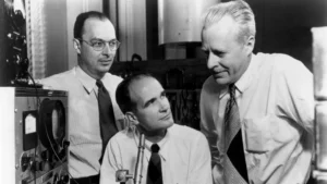
In 1947, a groundbreaking innovation emerged from the laboratories of Bell Labs, forever changing the course of electronics. Physicists John Bardeen and Walter Brattain successfully crafted the first functioning point-contact transistor, a pivotal achievement in the realm of semiconductors.
This heralded the birth of a revolutionary technology, profoundly impacting the trajectory of electronic components and circuitry.
Read More: Who invented Transistor, Really??
The point-contact transistor, constructed using a germanium crystal and delicate wire contacts, marked a departure from the vacuum tube technology prevalent at the time. This diminutive device paved the way for a new era of miniaturization, efficiency, and reliability in electronic circuit design.
Its significance lay in its ability to amplify electrical signals and act as a switch, laying the foundation for what would eventually become the heart of modern electronics.
2. Invention of First Integrated Circuit(1958)
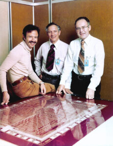
In 1958, at Texas Instruments, engineers Jack Kilby and Robert Noyce independently made a groundbreaking discovery. They invented the integrated circuit (IC), a pivotal moment in electronics. This innovation transformed electronic design and set the stage for the VLSI revolution.

Jack Kilby, a physicist at Texas Instruments, demonstrated the first working IC on September 12, 1958. He fabricated a simple circuit by depositing germanium thin-film resistors and capacitors on a single piece of semiconductor material.
This integrated circuit showcased the potential of integrating multiple electronic components into a compact, interconnected unit.
Around the same time, Robert Noyce, co-founder of Intel Corporation, was independently working on a similar concept.
Noyce envisioned a more practical and scalable approach to integrated circuits. Specifically, he advocated for using silicon instead of germanium, allowing for greater potential for mass production.
3. Invention of MOSFET
The Metal-Oxide-Semiconductor Field-Effect Transistor (MOSFET) is a key semiconductor device that has had a profound impact on modern electronics and is foundational to the field of VLSI (Very Large Scale Integration). The MOSFET was invented and developed through collaborative efforts over several decades, involving multiple researchers and contributions.
The origins of the MOSFET can be traced back to the 1920s and 1930s, with early work on semiconductor physics and transistors. However, it was only in the 1950s and 1960s that significant advancements were made in MOSFET technology.
In the early 1950s, Egyptian engineer Mohamed Atalla and Korean engineer Dawon Kahng, working at Bell Labs, began researching semiconductor surface properties. In 1959, they demonstrated the first functional MOSFET, outlining its potential for amplifying and switching electronic signals. This pivotal demonstration showcased the viability of MOSFET technology for practical applications.
Thanks to MOSFET advantages, such as high input impedance, low power consumption, and ease of miniaturization, propelled its adoption in the emerging field of integrated circuits. Consequently, by the mid-1960s, MOSFETs were a critical component in the early development of integrated circuits.
Over subsequent years, MOSFET technology continued to evolve, leading to refinements in fabrication processes, performance enhancements, and the development of complementary MOS (CMOS) technology. Today, MOSFETs are the fundamental building blocks of modern VLSI chips, enabling the integration of millions to billions of transistors on a single silicon chip.
4. Invention of CMOS
The Complementary Metal-Oxide-Semiconductor (CMOS) technology, a cornerstone of modern VLSI design, originated in the 1960s. It was a significant advancement in semiconductor technology, offering low power consumption, high noise immunity, and scalability.
He published a paper titled “PMOS and NMOS Inverters for MOS LSI” in which he outlined the basic principles of CMOS logic gates and their advantages.

Read More: CMOS: From Overlooked Innovation to Semiconductor Dominance
However, in the early 1970s, researchers at RCA (Radio Corporation of America), including Chih-Tang Sah and Mohamed Atalla, made notable progress in developing practical CMOS technology.
They refined the manufacturing processes and demonstrated the viability of CMOS as a cost-effective and low-power alternative to existing transistor technologies.
Following this progress, by the mid-1970s, the advantages of CMOS technology became widely recognized. Major semiconductor companies began adopting it for various applications, signifying a shift in the industry. Notably, the advent of CMOS marked a significant milestone in VLSI design.
This allowed for the integration of a vast number of transistors on a single chip while consuming minimal power, setting the stage for a technological revolution.
How were ICs designed before computers
Before the advent of computer-aided design (CAD) tools, the design of integrated circuits (ICs) was a highly manual and meticulous process. Engineers and designers relied on analog methods to create and verify IC designs. Now, let’s delve into an overview of the traditional IC design process before the integration of computer tools:
Conceptualization and Schematic Design:
Engineers would conceptualize the circuit and create a schematic diagram of the IC’s functionality, specifying the connections and components required.
Transistor-Level Design:
At the transistor level, designers would manually determine how the transistors should be connected to achieve the desired functionality, considering parameters like transistor sizes, voltage levels, and signal flow.
Layout Design:
Designers would hand-draw the physical layout of the IC on specialized graph paper or mylar sheets. They used templates and stencils for common structures and shapes. The layout involved placing and interconnecting transistors, resistors, capacitors, and other components according to the schematic.
Verification and Checking:
Designers would meticulously check the drawn layout against the schematic to ensure accuracy and adherence to design rules. This process often involved using magnifying glasses to scrutinize the tiny details of the layout.
Rule Checking:
The layout was manually checked against design rules and specifications to verify compliance. These rules included minimum feature sizes, spacing, and other fabrication constraints.
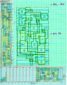
Rubylith Cutouts:
The final layout, once verified, was often transferred to rubylith sheets. Afterward, designers would cut out the design components and traces from the rubylith sheets—these were red-orange acetate sheets—and arrange them to represent the final IC layout.
Pasting and Final Verification:
The cut-out rubylith pieces were pasted onto a board or film to create a composite representation of the IC’s layout. Subsequently, designers would meticulously inspect and verify this physical representation to catch any errors in cutting, pasting, or peeling.

Photomasking and Manufacturing:
The final validated layout was used to create masks for photolithography, a crucial step in the manufacturing process, where the IC’s physical structure is defined on silicon wafers.
The manual nature of this process was time-consuming and prone to human errors, as demonstrated by the Intel 3101 64-bit RAM incident you mentioned. The advent of CAD tools revolutionized this process, significantly improving efficiency, accuracy, and design complexity in IC development.
What is Very Large Scale Integration
VLSI stands for Very Large Scale Integration, a field of semiconductor technology that involves combining thousands to billions of transistors on a single chip. VLSI technology allows for the creation of complex and highly functional integrated circuits (ICs) that serve as the building blocks for various electronic devices.
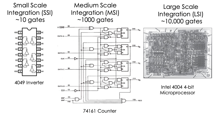
In VLSI design, transistors and other electronic components are miniaturized and integrated onto a semiconductor material, typically silicon. The goal is to optimize the performance, power efficiency, and size of the resulting integrated circuits.
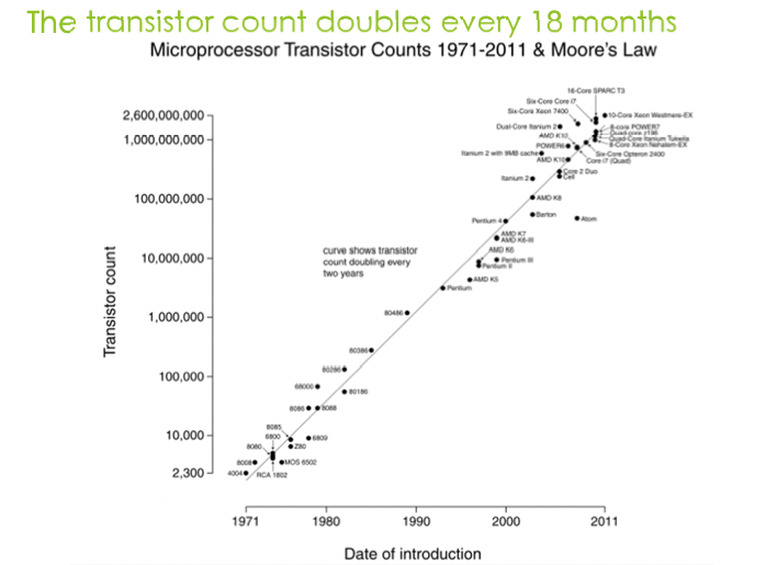
Moore’s Law has driven the VLSI Industry
Moore’s Law is the observation that the number of transistors in an integrated circuit (IC) doubles roughly every two years.
This observation and projection are based on historical trends, and it’s not a law of physics but rather an empirical relationship tied to production experience.
What are the 5 concerns for VLSI Industry as of today
1. Slow Memory in Semiconductor
2. Higher Frequency in Semiconductor
3. Untenable Power in semiconductor
4. ILP (Instruction-Level Parallelism)
5. Hard Network
Read more: 5 Major Challenges Faced by Semiconductor Industry
And off to Siliconomy
In today’s rapidly evolving digital landscape, we are witnessing the birth and growth of a new economy, the “siliconomy.”
Processing power now extends beyond traditional computing devices, reaching every aspect of our lives—the Siliconomy’s omnipresence. At its core is Intel, akin to the foundational silicon processor.
This term embodies technology’s transformative might, embracing five key superpowers: Compute, Connectivity, Infrastructure, Sensing, and AI. These superpowers redefine our world and interactions, reshaping lives and businesses. This blog post explores each superpower’s impact, unraveling their driving force within the siliconomy.

You can Read the History Section of Techovedas for more detailed insights into the rich Past of VLSI.
Cut to 2023
- 2nm Chip Design Costs $725 Million: Can the Industry Afford It?
- What is EUV that made ASML the biggest company of Europe
- How TSMC & ASML Monopolised the world?