Introduction:
The semiconductor industry stands as a testament to human ingenuity, continually pushing the boundaries of what’s possible in electronics and computing. At the heart of this innovation are patents—legal protections that recognize and reward groundbreaking discoveries and inventions. Throughout history, several patents have left an indelible mark on the semiconductor Industry, shaping the way we live, work, and communicate.
In this article, we delve into the top 10 patents that have significantly impacted the semiconductor industry. From the foundational planar transistor to cutting-edge FinFET technology, each patent represents a milestone in the evolution of semiconductor devices.
We’ll explore the problems these patents addressed, how they revolutionized semiconductor technology, and their lasting impact on the world of electronics.
Follow us on Linkedin for everything around Semiconductors & AI
10 Patents Which Revolutionized the Semiconductor Industry (Part 1)
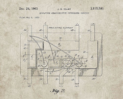
1. Planar Transistor (US Patent 2,901,477) – 1954, by Jack Kilby at Texas Instruments:
Problem that was being faced:
Before the invention of the planar transistor, electronic devices relied on bulky vacuum tubes, limiting the miniaturization and efficiency of electronic circuits. As technology advanced, the need for smaller, more reliable components became increasingly apparent.
How did the patent solve this problem?
Jack Kilby’s invention of the planar transistor revolutionized the semiconductor industry by introducing a compact, reliable alternative to vacuum tubes. By fabricating transistors on a single piece of silicon, Kilby’s patent laid the groundwork for the development of integrated circuits (ICs). This allowed for the miniaturization of electronic components and the creation of more complex circuits on a smaller scale.
What was the impact?
The impact of Kilby’s planar transistor patent cannot be overstated. It paved the way for the development of microprocessors, which are the heart of modern computing devices. The miniaturization made possible by the planar transistor led to the exponential growth of computing power and the proliferation of electronic devices in various industries, from telecommunications to consumer electronics. Kilby’s patent fundamentally changed the way we interact with technology and laid the foundation for the digital age.
Read More: 13 Semiconductor Terms Everyone MUST Know
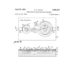
2. Integrated Circuit (US Patent 3,138,543) – 1959, by Robert Noyce at Fairchild Semiconductor:
Problem that was being faced:
Engineers constructed early electronic circuits using discrete components like transistors, resistors, and capacitors, connecting them on circuit boards. However, this approach limited the size and complexity of circuits, impeding further advancements in electronic technology.
How did the patent solve this problem?
Robert Noyce’s invention of the integrated circuit (IC) revolutionized electronics by consolidating multiple electronic components onto a single semiconductor substrate. This allowed for the creation of complex circuits with a much smaller footprint, leading to significant improvements in performance, reliability, and power efficiency.
What was the impact?
Noyce’s patent for the integrated circuit laid the foundation for modern semiconductor technology and fueled the rapid advancement of the electronics industry. ICs enabled the development of computers, smartphones, medical devices, and countless other electronic devices that have become integral to our daily lives. Noyce’s invention marked the beginning of the era of miniaturization, paving the way for the digital revolution.
Read more: 10 Pivotal Milestones in Semiconductor History
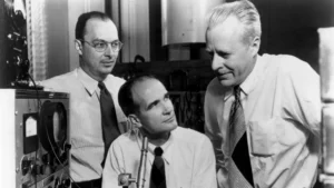
3. MOS (Metal-Oxide-Semiconductor) Transistor (US Patent 3,060,014) – 1962, by John Atalla and Dawon Kahng at Bell Labs:
Problem that was being faced:
Early transistor technology faced limitations in terms of size, speed, and power efficiency, hindering further advancements in electronic devices.
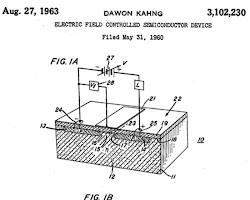
How did the patent solve this problem?
John Atalla and Dawon Kahng’s invention of the MOS transistor introduced a more efficient and versatile alternative to existing transistor technologies. The MOS transistor’s structure allowed for smaller, faster, and more energy-efficient transistors, laying the groundwork for the development of modern CMOS technology.
What was the impact?
The MOS transistor revolutionized the semiconductor industry and became the building block for the majority of digital integrated circuits (ICs) used today. Its low power consumption and high integration density made possible by the MOS transistor enabled the development of portable electronics, such as smartphones and laptops, as well as high-performance computing systems. Atalla and Kahng’s patent continues to influence technological innovation and drive progress in the semiconductor industry.
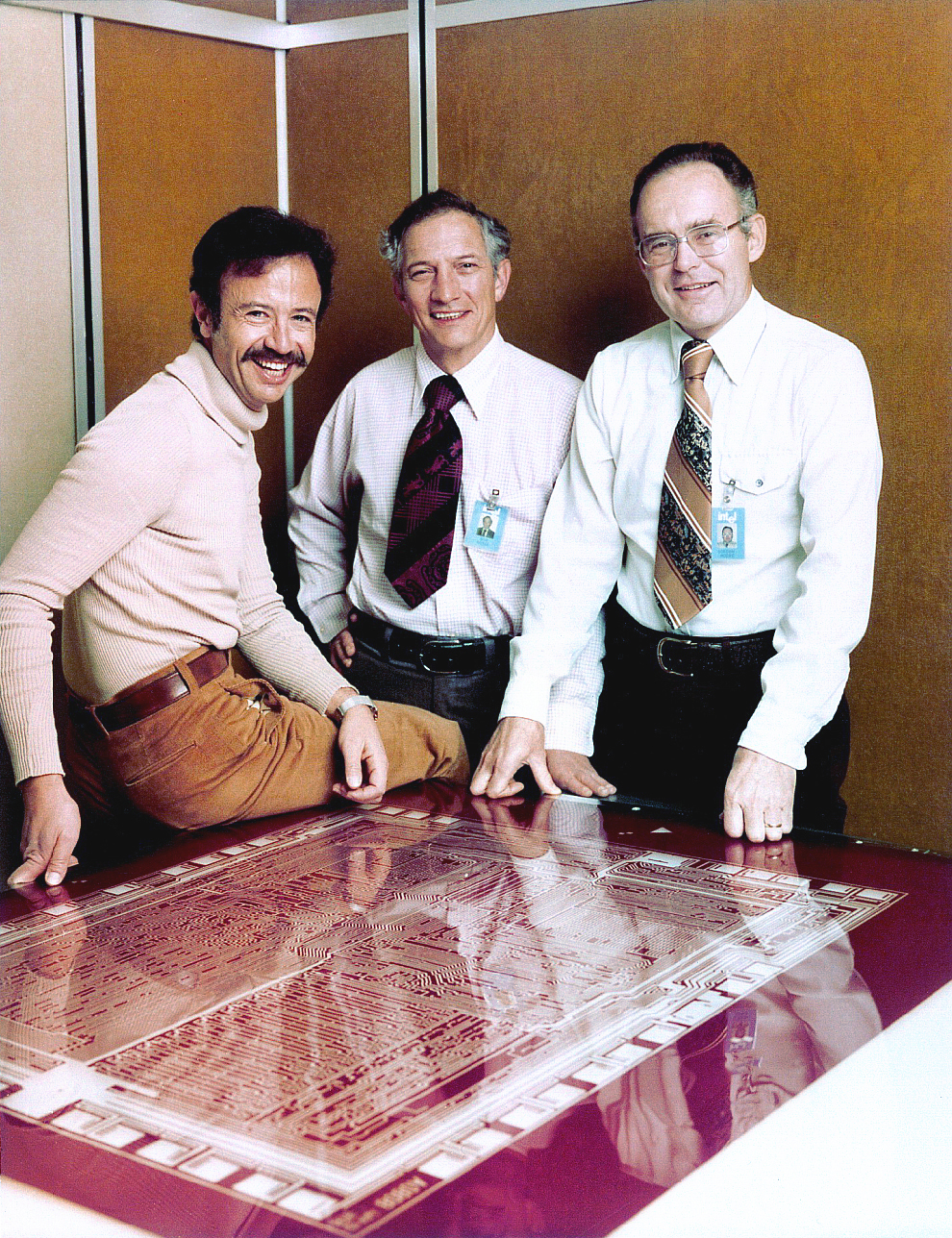
4. Local Oxidation of Silicon (LOCOS) process (US Patent 3,860,006) – 1975, by Jean Hoerni at IBM:
Problem that was being faced:
Creating isolated regions of oxide on a silicon wafer for building complex integrated circuits (ICs) with multiple transistors was challenging and limited the scalability of semiconductor devices.
How did the patent solve this problem?
Jean Hoerni’s invention of the Local Oxidation of Silicon (LOCOS) process provided a reliable and scalable method for creating isolated regions of oxide on a silicon wafer. This allowed for the fabrication of complex ICs with multiple transistors in close proximity without interference.
What was the impact?
The LOCOS process revolutionized semiconductor manufacturing by enabling the production of more advanced and densely packed integrated circuits. This led to the development of smaller, faster, and more powerful electronic devices, ranging from microprocessors to memory chips. Hoerni’s patent played a crucial role in the evolution of the semiconductor industry and continues to be a cornerstone of modern IC fabrication processes.
5. Shallow Ion Implantation (US Patent 4,093,871) – 1978, by Arthur Ashkin and Richard Lee at Bell Labs:
Problem that was being faced:
Precisely doping silicon wafers with impurities to control the electrical properties of transistors was challenging and limited the miniaturization of electronic devices.
How did the patent solve this problem?
Arthur Ashkin and Richard Lee’s invention of shallow ion implantation provided a precise method for doping silicon wafers with impurities, enabling better control over transistor characteristics. This technique allowed for the continued miniaturization of transistors according to Moore’s Law.
What was the impact?
Shallow ion implantation revolutionized semiconductor manufacturing by providing a more precise and controllable method for doping silicon wafers. This enabled the production of smaller, faster, and more energy-efficient transistors. The new technique drove advancements in electronic devices such as microprocessors and memory chips. Ashkin and Lee’s patent remains an essential technology in semiconductor fabrication processes.
Part 2 will talk about the next 5 Patents. Read here
Conclusion:
Innovation in the semiconductor industry is a story of perseverance, creativity, and collaboration. The patents highlighted in this article have played pivotal roles in driving technological progress and shaping the modern world. Transistor miniaturization pioneered advancements. Three-dimensional transistor structures followed suit. These inventions enabled smaller, faster, and energy-efficient devices. The spirit of innovation in these patents will drive the semiconductor industry forward.
New challenges will emerge, and new solutions will be devised, driving further advancements in electronics, computing, and beyond.