Introduction
In the ever-evolving landscape of semiconductor technology, advanced packaging has emerged as a pivotal bridge between semiconductor manufacturing and packaging. This innovative approach integrates diverse functionalities into a single package, revolutionizing the traditional boundaries of semiconductor design and assembly.
Let’s delve into how advanced packaging is reshaping the semiconductor industry by seamlessly merging manufacturing and packaging processes.
Follow us on Linkedin for everything around Semiconductors & AI
Semiconductor Manufacturing and Packaging
Semiconductor manufacturing and packaging are two distinct processes within the semiconductor industry, each serving crucial roles in the production of electronic devices.
To understand their differences using an analogy, let’s consider the process of baking a cake.
Semiconductor Manufacturing: This process is analogous to preparing the ingredients for the cake, mixing them together, and baking the cake itself. In semiconductor manufacturing, engineers prepare silicon wafers by creating intricate patterns of electronic components using processes such as photolithography, etching, and doping.
This is akin to mixing ingredients like flour, sugar, eggs, and baking powder in precise quantities to form the cake batter. Just as the cake batter undergoes baking to solidify and form the cake, the silicon wafer undergoes various treatments to create transistors, capacitors, and other components on its surface.
Packaging: Packaging in semiconductor production is comparable to decorating and packaging the baked cake. After fabricating the semiconductor components on the silicon wafer, manufacturers must protect, connect, and organize them to facilitate their integration into electronic devices.
Packaging involves encapsulating the semiconductor chip in a protective material, connecting it to external circuitry via wire bonding or flip-chip bonding, and sometimes adding additional layers for thermal dissipation or mechanical support.
This is like frosting the cake, placing it on a decorative plate, and perhaps wrapping it in a box or placing it in a cake stand for presentation and transport.
Read More: 3 Lesser Known Semiconductor Stocks Which Can 5X Your Investment by 2030 – techovedas
What is the technical Difference between Semiconductor Manufacturing and Packaging
Semiconductor Manufacturing:
- Semiconductor manufacturing, also known as fabrication or “fab” for short, involves the creation of integrated circuits (ICs) or chips on a silicon wafer.
- This process includes several intricate steps such as photolithography, etching, doping, deposition, and polishing.
- Photolithography is a key step where a pattern is transferred onto the wafer using light-sensitive materials, defining the circuitry of the chip.
- Etching involves removing material from the wafer according to the pattern defined by photolithography.
- Doping introduces specific impurities into the silicon to alter its electrical properties, essential for creating transistors and other semiconductor components.
- The result is a wafer with multiple layers of electronic components fabricated on its surface.
Packaging
- Packaging, also referred to as assembly and test, occurs after semiconductor manufacturing and involves preparing the individual chips for integration into electronic devices.
- The packaged chip includes the IC, as well as necessary connections, protection, and thermal management features.
- Packaging serves several purposes including providing electrical connections between the chip and external circuitry, protecting the chip from environmental factors such as moisture and mechanical stress, and dissipating heat generated during operation.
- Common packaging techniques include wire bonding, flip-chip bonding, and encapsulation in materials such as plastic or ceramic.
- Wire bonding involves connecting the chip to external leads using thin wires, while flip-chip bonding involves directly connecting the chip to a substrate using solder bumps.
- Once packaged, the chips undergo testing to ensure they meet performance specifications and reliability standards.
In essence, semiconductor manufacturing focuses on creating the electronic components on a silicon wafer, while packaging involves preparing these components for integration into electronic devices by providing electrical connections, protection, and thermal management. Both processes are essential steps in the semiconductor production chain, with each contributing to the functionality, reliability, and performance of electronic devices.
Read More:India’s First Semiconductor Fab to Begin Production by 2026 – techovedas
How Advanced Packaging is blurring the Lines of Semiconductor Manufacturing and Packaging?
Advanced packaging techniques are indeed blurring the lines between semiconductor manufacturing and packaging by integrating some aspects of both processes. Here’s how advanced packaging is achieving this merger:
System Integration on Package (SiP):
- SiP involves integrating multiple semiconductor dies, including processors, memory, and other components, onto a single package.
- This integration often includes heterogeneous integration, where different types of dies are combined, such as logic, memory, and sensors.
- SiP allows for more efficient use of space, reduced interconnect lengths, and improved performance compared to traditional separate packaging of individual components.
- In System-in-Package (SiP), manufacturers fabricate components separately using semiconductor manufacturing techniques, but they actively integrate them onto the same package during the packaging process, effectively blurring the lines between manufacturing and packaging.
Read More: How Advanced Packaging is Merging Semiconductor Manufacturing and Packaging – techovedas
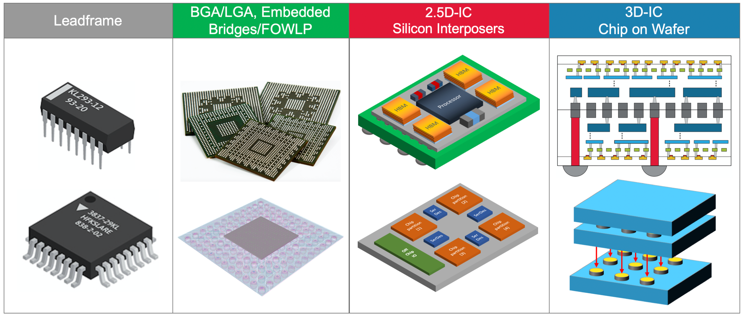
3D Packaging:
- 3D packaging involves stacking multiple layers of semiconductor dies vertically, connected through through-silicon vias (TSVs) or other interconnects.
- This technique enables higher levels of integration and functionality in a smaller footprint, improving performance and energy efficiency.
- In 3D packaging, individual dies are manufactured separately, but they are stacked and interconnected during the packaging process, merging aspects of both manufacturing and packaging.
Wafer-level Packaging (WLP):
- WLP involves packaging semiconductor dies while they are still part of the wafer, before they are singulated into individual chips.
- This approach reduces manufacturing costs and improves yields by packaging multiple dies simultaneously.
- WLP blurs the line between semiconductor manufacturing and packaging by integrating packaging steps into the wafer fabrication process itself.
Embedded Die Packaging:
- Embedded die packaging involves embedding semiconductor dies directly into a substrate or carrier material, such as organic or ceramic substrates.
- This technique reduces the footprint of the package and improves thermal performance by embedding the dies closer to the substrate.
- Embedded die packaging combines aspects of both semiconductor manufacturing (die fabrication) and packaging (embedding into a substrate).
These advanced packaging techniques leverage the capabilities of both semiconductor manufacturing and packaging processes to achieve higher levels of integration, performance, and functionality in electronic devices. By merging aspects of both processes, advanced packaging enables the development of more compact, efficient, and capable semiconductor packages for a wide range of applications.
Read More: India’s First Semiconductor Fab to Begin Production by 2026 – techovedas
Conclusion
As advanced packaging continues to evolve, it not only enhances the efficiency of semiconductor manufacturing but also enables the development of increasingly sophisticated and compact electronic devices.
By merging manufacturing and packaging processes, this transformative approach promises to drive further advancements in semiconductor technology, shaping the future of electronics across industries.