Introduction:
Imagine the inner workings of your smartphone, laptop, or even that trusty toaster. At the heart of these devices lies an unsung hero: the Printed Circuit Boards (PCBs).
PCBs are the foundation upon which modern electronics are built. These thin, layered boards contain a network of electrical pathways that connect various electronic components, allowing them to communicate and function together.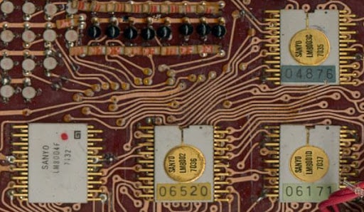
The journey of Printed Circuit Boards (PCBs) unfolds as a captivating narrative of innovation and technological progress.
From their humble beginnings to their pervasive presence in modern electronics, PCBs have revolutionized the way we interact with technology.
Moreover, this comprehensive exploration delves into key milestones and pivotal moments that have shaped the evolution of PCBs over more than a century.
Follow us on Linkedin for everything around Semiconductors & AI
The Birth of Electricity (1880-1900):
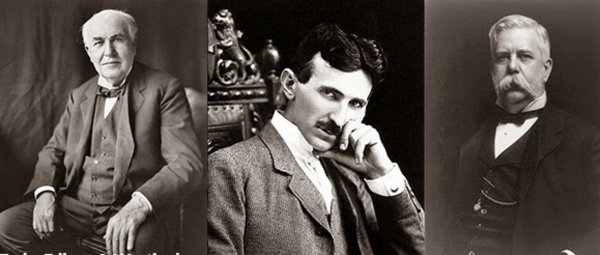
The late 19th century witnessed a transformative shift with the advent of electricity. Innovators like Thomas Edison, Nikola Tesla, and Alexander Graham Bell spearheaded groundbreaking discoveries, laying the groundwork for the electrification of society.
Their inventions not only illuminated homes and powered machinery but also set the stage for the future integration of electronic components on PCBs.
Read More: UK’s First 300mm Wafer Fab: Giant Chip Factory for Ultra-Thin Flex ICs – techovedas
Evolution of PCBs
The evolution of Printed Circuit Boards (PCBs) represents a remarkable journey from simple electrical connections to complex, high-performance substrates that underpin modern electronic devices. 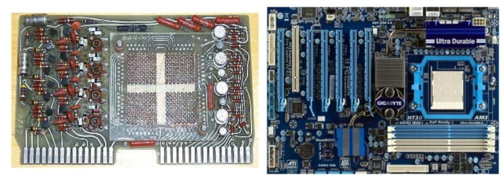
This article explores the key stages in the evolution of PCB technology, highlighting significant advancements and innovations that have shaped its development over time.
Actually, the beginning ideas for the PCB weren’t invented during this era. However, without the manufacturing progress of The Gilded Age, and also the spreading influence of electricity, the PCB would never be what it’s today.
The Emergence of PCB Concepts (1890-1920):
Albert Hanson’s patent filing in 1903 marked a significant milestone in the evolution of PCBs. His vision of integrating conductive traces on insulating substrates foreshadowed the concept of modern-day Printed Circuit Boards (PCBs) 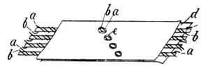
The First Albert Hanson PCB patent drawing
Hanson’s pioneering work laid the foundation for subsequent innovations, albeit in rudimentary forms, and paved the way for the widespread adoption of PCB technology.
Read More: What are Top 7 Customers of TSMC in 2023 – techovedas
World War II and PCB Adoption (1930-1945):
1920s:
During the 1920s, while innovative household appliances like washing machines, vacuums, and refrigerators were introduced, the integration of PCBs into these devices had not yet occurred.
However, a significant milestone in PCB history was achieved in 1925 when Charles Ducas invented a patent detailing the addition of conductive inks to an insulating material.
Although initially used for flat heating coils, Ducas’ patent laid the foundation for the development of printed wiring boards (PWBs), marking a crucial step toward the modern PCB technology we know today.
Read More: Twice the Speed, Half the Power of Nvidia’s H100: Intel Releases AI Chip Gaudi 3 – techovedas
1930-1945:
The period spanning from the 1930s to 1945 was marked by the outbreak of World War II, a time of significant advancement in PCB technology.
Additionally, PCBS found their first practical application in the proximity fuse, a crucial innovation for high-velocity artillery shells that required precise firing over long distances.
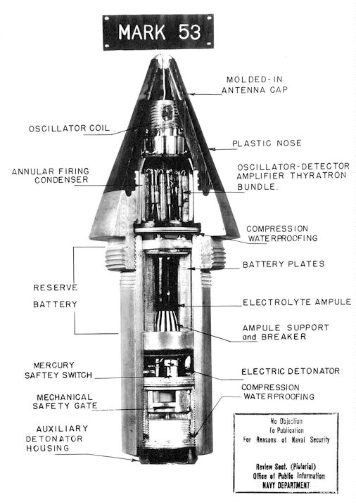
Proximity fuse was the first military application to use a PCB
Invented by the British, the proximity fuse utilized PCB technology, demonstrating its effectiveness in military applications. Concurrently, Paul Eisler, an Austrian residing in the UK, filed a patent for copper foil on a non-conductive base during this period.
This concept, akin to modern PCB manufacturing methods, laid the groundwork for future advancements in PCB technology.
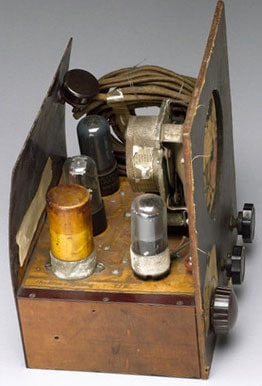
A radio made by Paul Eisler that uses first printed circuit board (PCB)
Eisler’s pioneering work further advanced PCB development when he successfully created a radio incorporating a PCB in 1943, showcasing the potential for PCBs in military and civilian applications alike.
Read More: Nvidia, Amazon Pour $110 Million into AI with US- Japan University Alliance – techovedas
1940s:
Despite notable advancements in household appliances such as vacuum cleaners, washing machines, televisions, and radios during the 1940s, the widespread integration of consumer-level PCBs had not yet occurred.
Paul Eisler’s groundbreaking work on PCBs had not yet permeated consumer electronics, as evidenced by the absence of PCBs in devices like the Motorola television from 1948. 
An old Motorola television from without PCB in 1948
Although electronic devices continued to evolve during this decade, the underlying foundation of PCB technology had not yet become commonplace in consumer products, indicating that further advancements were needed to fully realize the potential of PCBs in everyday electronics.
Read More: UK’s First 300mm Wafer Fab: Giant Chip Factory for Ultra-Thin Flex ICs – techovedas
The Golden Age of PCBs (1947-1970):
Post-war prosperity ushered in an era of unprecedented innovation in PCB technology. Milestones such as plated through-hole technology and surface mount technology revolutionized manufacturing processes, enabling the mass production of intricate electronic assemblies. The space race and advancements in computing drove demand for high-performance PCBs, fueling rapid industry growth.
1947-1970:
PCBs underwent significant advancements during this period, as the US Army’s patent for the “Processing of Assembling Electrical Circuits” in 1956 revolutionized electronic assembly techniques by introducing copper traces.
The Space Race rivalry between the USA and Russia spurred further developments in PCB technology, particularly in aerospace applications where reliability and miniaturization were paramount.
In 1963, Hazeltine Corporation introduced plated through-hole technology, a milestone that revolutionized the electronics industry. Moreover, this innovation enabled denser component placement and enhanced electrical connectivity, pivotal for the burgeoning electronics industry.
Concurrently, IBM’s innovation in Surface Mount Technology (SMT) paved the way for more compact and efficient PCB designs, particularly notable in the construction of Saturn rocket boosters, where space optimization was critical.
Read More: OpenAI: A Chronology of Events from Humble beginnings to AI Superpower
1970s:
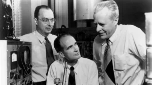
The emergence of microprocessors in the 1970s revolutionized the electronics landscape, enabling the integration of complex circuitry onto single integrated circuits (ICs), fundamentally altering the role of PCBs in facilitating connectivity.
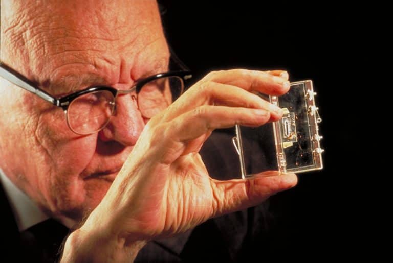
Jack Kilby is holding the first integrated circuit
This era witnessed a significant shift towards miniaturization and increased complexity in electronic devices, necessitating more sophisticated PCB designs capable of accommodating intricate circuit configurations.
As the demand for electronic devices grew, PCB manufacturing processes became more refined and standardized, contributing to improved reliability and performance of electronic systems across various industries.
Read More: iPhone Production Doubles to $14 Billion in India: 1 in 7 iPhones Now Made in India – techovedas
1980s:
The Digital Age of the 1980s saw the proliferation of personal electronic devices such as CDs, VHS players, and gaming consoles, driving demand for more advanced PCB designs capable of supporting these technologies.
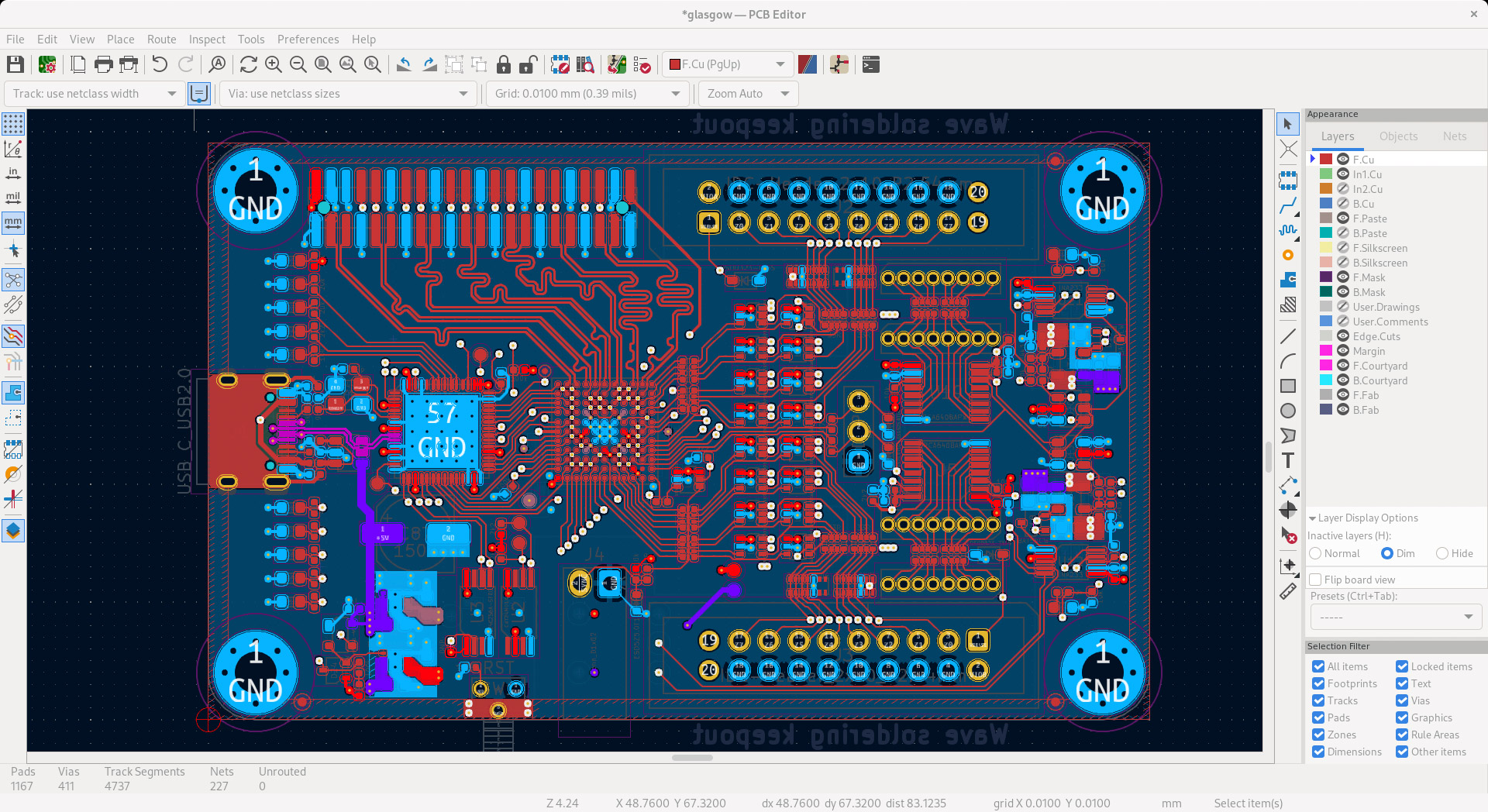
Computer-aided design (CAD) software revolutionized PCB design practices, enabling engineers to create more intricate layouts with greater precision and efficiency, marking a significant departure from traditional hand-drawn methods.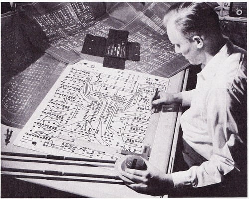
Drawing a PCB with tape and mylar before EDA arrived
Additionally, advancements in manufacturing processes and materials during this period further enhanced the quality and reliability of PCBs, laying the foundation for future innovations in electronic design and production.
Read More: OpenAI Seeks Billions of Funds to Build Chip Factories – techovedas
The 1990s – The Internet Age
The 1990s witnessed a surge in silicon technology, with the introduction of Ball Grid Arrays (BGAs) and the integration of memories and Systems on Chip (SoC) into PCBs, such as driving increased functionality and performance in electronic devices.
Design for Test (DFT) strategies became essential as electronic components continued to shrink in size, requiring careful consideration of accessibility and testability during PCB layout and assembly.
Moreover, the widespread adoption of surface mount technology (SMT) and advancements in assembly processes enabled manufacturers to produce PCBs with higher component densities and improved reliability, fueling further innovation in electronic design and manufacturing.
Read more: Top 10 Semiconductor Companies in India and Why They’re Poised for Growth – techovedas
2000s & Beyond:
The 2000s marked a period of transition and innovation in PCB design, as the industry grappled with an aging workforce and the emergence of new technologies such as wearables and wireless communication.
Additionally, Flexible circuitry and advanced materials opened up new possibilities for PCB design, enabling the development of more compact and versatile electronic devices with enhanced functionality.
Looking ahead, the future of PCB design holds promise for continued advancements in areas such as photonics and wireless connectivity, as engineers strive to meet the evolving demands of the digital age.
Read More: 5 Videos Delving into the Dark Side of Semiconductor Dreams – techovedas
Conclusion:
The history of PCBs is a testament to human ingenuity and the relentless pursuit of progress. From their humble origins to their ubiquitous presence in modern electronics, PCBs have transformed the way we live, work, and communicate. As we look ahead to the future,
Moreover, PCBS will continue to play a vital role in driving innovation and shaping the technological landscape for generations to come.