Introduction
Taiwan Semiconductor Manufacturing Company (TSMC) has been making ripples in the semiconductor industry with its quest to make transistors smaller. TSMC’s recent revelation in its 2023 annual report marks a pivotal moment as the company delves into the Angstrom Age with the A14 production process, a technological leap that promises enhanced speed, power, density, and cost efficiency.
As the semiconductor industry anticipates TSMC’s unveiling of A14 details at the 2024 Technology Symposium, the anticipation for the future of semiconductor technology is at an all-time high.
Angstrom Age: Currently, chip manufacturing operates in the nanometer (nm) scale. A single nanometer is equal to one billionth of a meter. The A14 process takes things a step further, venturing into the angstrom (Å) scale, which is ten times smaller than a nanometer.
This translates to significantly denser transistors on a chip, paving the way for exponential performance gains.
Performance Boost: With this much tighter packing of transistors, we can expect significant improvements in chip performance.
Early estimates suggest the A14 process could deliver dramatic leaps in processing power and energy efficiency compared to current-gen chips.
Timeline: While the exact details are still under wraps, reports suggest TSMC might begin trial production of the A14 process in facilities around Kaohsiung, Taiwan, as early as 2027.
This indicates commercially available chips utilizing this technology might be a few years down the line.
Read more TSMC to Build 1nm Transistors by 2030 – techovedas
TSMC’s enters into A14 process
The A14 technology, boasting a 14 angstroms (or 1.4-nanometers) feature size, demonstrates the company’s relentless pursuit of innovation in semiconductor manufacturing.
Targeted at both System on Chip (SoC) and High-Performance Computing (HPC) applications, the A14 process follows the 2nm production, slated to enter mass production in 2025.
TSMC’s ambitious exploratory studies also extend towards nodes beyond A14, solidifying their commitment to pushing the boundaries of technological advancement.
Bringing 2nm to mass production and developing A14 and beyond processes increased the R&D budget.
Read more 7 Pillars of TSMC Roadmap to Chip Supremacy Till 2030 – techovedas
Research and Development Advancements
TSMC’s fervent dedication to research and development is evident in the impressive 11.7% year-on-year increase in its R&D budget for 2023.
The substantial allocation of resources towards R&D, totalling NT$182.4 billion (US$5.96 billion), reflects TSMC’s relentless pursuit of pushing the envelope in advanced processes.
It further reinforces their steadfast focus on pioneering technologies such as the 2nm platform, A14 and beyond, 3D-IC front-end packaging/integration, next-generation lithography, and long-term explorations into specialty SoC technologies and transistors with an 8 to 10-year horizon.
R&D is focused on TSMC’s bread & butter
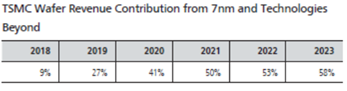
TSMC’s strategic advancements in advanced processes, particularly those of 7nm-and-below, have translated into significant revenue growth. In 2023, these advanced processes accounted for 58% of TSMC’s revenue, with projections for 2024 indicating an increase to 60-70% of the total revenue. Total 2024 shipments are forecast at 13 million to 14 million wafers (12-inch equivalent).
Furthermore, TSMC’s projected compound annual growth rate for the worldwide semiconductor market, excluding memory, from 2023 through 2028 stands at a notable high single-digit figure, reflecting a confident outlook for sustained growth and innovation in semiconductor technology.
Read more 5 Major Takeaways from TSMC Impressive Q1 FY24 Results – techovedas
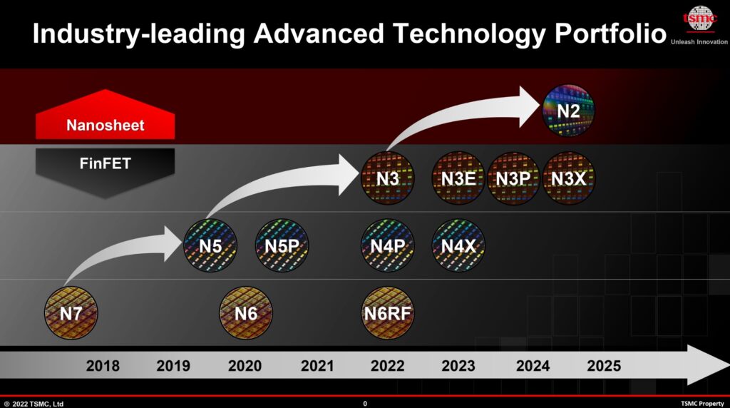
HPC and the N3 node
The trajectory of TSMC’s advancements aligns with the increasing demand for High-Performance Computing (HPC) solutions, driven by factors such as AI adoption and the proliferation of 5G technologies.
Currently, TSMC’s 3nm family is focused on high performance computing and mobile.
- N3E (Enhanced N3) for HPC and mobile, mass production in Q4 2023
- N3X (Tailored for HPC) mass production in 2nd half 2024
- N3AE (Automotive Early) for automotive, PDKs out now
TSMC forecasts low-single-digit growth in HPC unit shipments for 2024, reflecting the company’s strategic alignment with the burgeoning needs of an increasingly connected and intelligent world. This demand is fueling the development of higher performance and more power-efficient central processing units (CPUs), graphics processor units (GPUs), Neural Processing Units (NPUs), and AI accelerators, positioning TSMC as a central figure in shaping the future of HPC and related technologies.
Read more TSMC N3P To Outperform Intel 18A, Derailing Intel’s Foundry Leadership Plan by 2025 – techovedas
Innovative Packaging Solutions – CoWoS line up
TSMC’s prowess in advanced chip packaging is evident through the evolution of its CoWoS (Chip on Wafer on Substrate) technology. The development of CoWoS-S and CoWoS-L for HBM3e memory chip production, as well as the preparations for HBM4, mark significant strides in advancing packaging solutions.
CoWoS-S (CoWoS – Silicon Interposer)
This variant integrates multiple System-on-Chip (SoC) chips with HBM3 (High Bandwidth Memory 3) stacks using a silicon interposer. Mass production for CoWoS-S, featuring the specified silicon interposer size, will begin in 2023.
CoWoS-L (CoWoS – Local Silicon Interconnects)
This variant is under development for interposers larger than the 3.3-reticle size. It entails reconstituting interposers with multiple LSIs (Local Silicon Interconnects). Mass production for CoWoS-L is scheduled to start in 2024.
CoWoS-R (CoWoS – Redistribution Layer Interposer)
Tailored for enhanced signal integrity, specifically for High-Performance Computing (HPC) applications. Mass production for CoWoS-R started in 2023.
Additionally, the mass production of InFO (Integrated Fan-Out) solutions, such as InFO_oS Gen-5 and InFO_M_PoP. It showcases TSMC’s commitment to delivering innovative, high-bandwidth packaging solutions catering to diverse application requirements.
Read more CoWoS: TSMC’s New Secret Weapon for Advanced Packaging – techovedas
TSMC R&D focus in 2024
TSMC’s total R&D budget is estimated at around 8% of full-year 2024 revenue and aimed at:
- Advancing the 2nm platform.
- Developing the A14 process and exploring advancements beyond it.
- Improving 3D IC front-end packaging and integration. Researching next-generation lithography techniques.
- Long-term exploration of specialty SoC technologies like new NVM, MEMS, RF, and analog, with a horizon of 8 to 10 years.
Follow us on Linkedin for everything around Semiconductors & AI
Conclusion
In conclusion, TSMC’s entry into the A14 production process a new era of innovation . In semiconductor manufacturing, with a focus on advancing SoC and HPC applications.
The company’s robust R&D investments underscore its commitment to pushing the boundaries of technology. It’s evident in the pursuit of the 2nm platform, exploration beyond A14, and advancements in packaging solutions. It is like CoWoS and InFO.The silicon interposer for CoWoS-S should measure 3.3 reticles, using reticles, a unit in semiconductor manufacturing, for measurement. Mass production for CoWoS-S with the specified silicon interposer size will commence in 2023.
Read more What are Top 7 Customers of TSMC in 2023 – techovedas