Introduction
Your phone is a tiny powerhouse, but have you ever wondered how they fit so much computing power in your pocket? It’s all thanks to a concept called “technology node”. Technology node is the key ingredient that lets manufacturers build faster, more efficient phones without them needing to be any bigger.
Recently, there has been significant confusion surrounding the naming of advance technology nodes. In this article, we will explore what technology nodes are, what they represent, and the nomenclature significance in advanced nodes.
Follow us on Linkedin for everything around Semiconductors & AI
What is a technology node?
The technology node (also process node, process technology or simply node) refers to a specific semiconductor manufacturing process and its design rules. Different nodes often imply different circuit generations and architectures. Generally, the smaller the technology node means the smaller the feature size, producing smaller transistors which are both faster and more power-efficient.
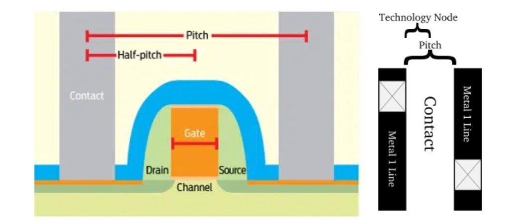
Historically, the process node name referred to a number of different features of a transistor including the gate length as well as M1 half-pitch. M1 here refers to metal layer 1. The fabrication of chips is done in multiple layers and the lowest metal layer is called metal 1.
Read more 8 Major Steps of Semiconductor Fabrication – techovedas
How did the term ‘node’ arise?
The term “node” in semiconductor technology originated from the half-pitch measurement of a DRAM chip’s memory cell. In the 1990s and early 2000s, microprocessor advancement prioritized higher frequencies. Meanwhile, DRAM progress aimed to meet the rising demand for larger capacities.
Since higher capacities were achieved through higher density, it was DRAM that became the driver of technology scaling. The node’s name typically aligns with half of the pitch, known as the “half-pitch,” of the active area in the memory cell array. The half-pitch of the memory cell in a DRAM chip is a crucial dimension influencing the chip’s overall capacity.
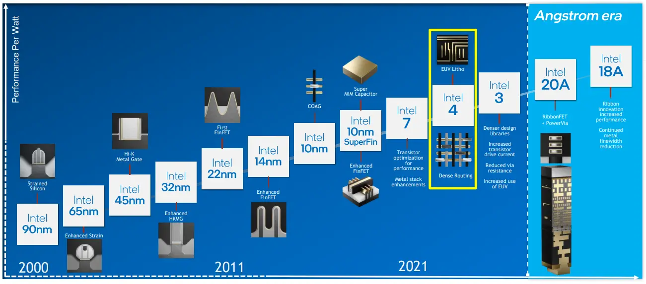
Timeline of tech nodes
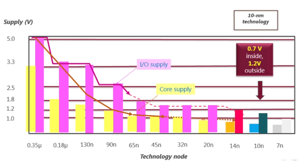
Early Days In the early days of semiconductor technology, the node name directly corresponded to certain physical dimensions of the transistors. For example, a 90nm node meant that the smallest feature on the chip was 90nm wide. The technology with a set of feature sizes of devices is called a technology node or generation, such as 0.35 μm technology node in the 1990.
Late 1990s In 1997, most of the leading semiconductor introduced the 250nm process node. The 180nm process node was introduced in 1999 by most Intel, Texas Instruments, IBM, and TSMC. This lasted until the 0.25 µm process in 1997 at which point Intel started introducing more aggressive gate length scaling. For example, their 0.25 µm process had Lg = 0.20 µm and likewise, their 0.18 µm process had Lg = 0.13 µm (a node ahead). At those nodes the “process node” was effectively larger than the gate length.
The term “node” emerged in the 1990s, aligning with the era of microprocessor development focused on achieving higher frequencies. Meanwhile, DRAM development prioritized meeting escalating demands for greater capacities. In recent years, the precise meaning of node numbers has blurred due to marketing and foundry discrepancies. Modern nodes like 22 nm, 16 nm, 14 nm, and 10 nm denote specific generations of chips manufactured using particular technologies.
Read more TSMC to Build 1nm Transistors by 2030 – techovedas
Evolution of FETs with technology nodes
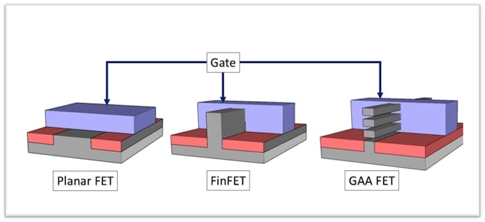
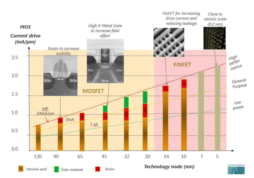
Starting from 22 nm technology, the technology has switched from MOSFETs to fin field effect transistor (FinFET). Scaling MOSFETs below 22nm faced challenges such as increased gate leakage, exacerbated short channel effects.
FinFETs revolutionized semiconductor design by introducing a 3D fin structure. This innovation enhanced gate control, curbing leakage and mitigating short channel effects. By enveloping the channel on three sides, FinFETs offered superior electrostatic management and thicker gate oxide layers, crucial for reducing leakage currents.
The architecture behind FinFET is in three-dimensional configuration . The term of gate length is no longer fit to describe the process technology. Nowadays, technology nodes such as 10 nm and 5 nm do not correspond to any gate length or half pitch distance anymore as the technology switched from planar structure to FinFET or Gate-all-around FET (GAA FET).
The transition from FinFETs to Gate-All-Around (GAA) FETs occurred around the 5nm technology node. Gate-All-Around (GAA) FETs provided enhanced control over the channel region by surrounding the channel with gate material on all sides. This 360-degree gate coverage provided superior electrostatic control.
Read more Samsung’s 3 nm Secret: GAA Transistors – techovedas
What are Mature nodes vs Advance nodes?
Generally, nodes with transistor feature sizes above 28nm are considered mature nodes. “Mature nodes” refer to well-established semiconductor manufacturing processes that have been optimized for mass production. These nodes typically have larger transistor feature sizes (e.g., 45nm, 28nm) and are used for producing a wide range of integrated circuits for various common applications such as consumer electronics, automotive, and industrial products.
“Advanced nodes,” on the other hand, represent the cutting-edge of semiconductor manufacturing technology. These nodes have smaller transistor feature sizes (e.g., 10nm, 7nm, 5nm) and enable the production of chips with higher transistor density, improved performance, and lower power consumption. Advanced nodes are typically used for manufacturing high-performance computing (HPC), artificial intelligence (AI), and other demanding applications.
Read more Chip Shortages Continue for Mature Nodes – Impacting Multiple Industries – techovedas
What is wrong with technology nodes 5nm 3nm 2nm?
The naming convention of “5nm”, “2nm”, “1nm” etc., in the context of transistors, has evolved over time. Initially, these technology nodes were named after the size of a specific transistor feature. For instance, the “32 nm” node, which began in 2010, featured transistors with an average gate length of less than 32 nanometers.
However, as technology advanced and transistors became smaller, the naming convention started to deviate from actual physical dimensions. The modern-day chipset nanometer technology refers to the improvement in the manufacturing process rather than the size of the transistor itself. It has now become more of a marketing term.
But then why do companies name it as 5nm?
This is because their device released with packaging and other optimizations is expected to perform like a 5nm device. The nm terminology is a simple way for semiconductor companies to convey the idea of progress and improvement to consumers.
Read more What is the Transistor Size of 2 nm Process Node ? – techovedas
Why are we going towards lower nodes?
- As technology nodes advance, the dimensions of transistors decrease, enabling a higher transistor density per unit area. This increase in transistor density aligns with Moore’s Law, as it enables the integration of more functionality onto a chip, contributing to the continuous improvement in computational power.
- Smaller transistors also typically offer higher performance due to shorter switching times and reduced power consumption.
- Advances in technology nodes often result in cost reductions per transistor. As manufacturers can fit more transistors onto a single chip without significantly increasing manufacturing costs, the cost per transistor decreases with each successive technology node.
Conclusion
In conclusion, while semiconductor technology nodes have undergone significant changes over time, their primary purpose remains facilitating high computation power and lowering power consumption. By embracing lower nodes and advancing semiconductor manufacturing, the industry continues to push the boundaries of what’s possible in electronics, driving forward technological development for a better future.